



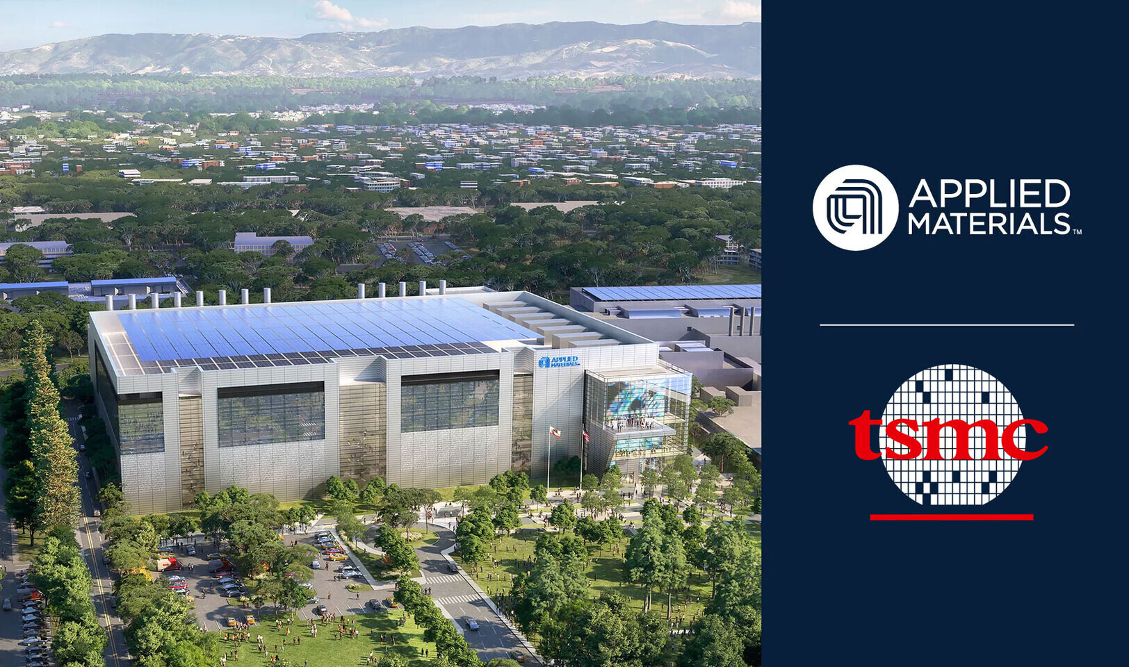
TSMC and Applied Materials are expanding their long running partnership with a new effort focused on the future of advanced chipmaking.
The companies will work together at Applied Materials’ EPIC Center in Silicon Valley, a $5 billion research and development hub built to speed up semiconductor equipment, materials, and process innovation.
The goal is to solve some of the hardest problems facing next generation AI chips. As chip designs move toward more complex 3D transistor structures, stacked architectures, and advanced interconnects, manufacturing becomes much harder. Materials engineering and process integration are now just as important as transistor design itself.
Applied Materials says the EPIC Center will help chipmakers move new technologies from early research to high volume manufacturing more quickly. TSMC will use the collaboration to work on equipment and process readiness for future chip nodes.
The partnership will focus on three major areas:
| Focus area | Why it matters |
|---|---|
| Advanced logic scaling | Helps improve power, performance, and area for future AI and HPC chips |
| New materials and equipment | Needed for complex 3D transistors and interconnect structures |
| Process integration | Improves yield, reliability, and variability control at advanced nodes |
This matters because AI chips are becoming harder to scale through traditional methods. Data centers need more performance, but they also need better energy efficiency. That puts pressure on foundries and equipment makers to improve every part of the manufacturing stack.
Applied Materials and TSMC have worked together for more than 30 years, but the EPIC Center gives them a more direct place to co develop future technologies. Applied says the site will give chipmakers earlier access to its R&D portfolio, faster learning cycles, and a secure environment for collaboration.
For TSMC, the partnership helps address the rising complexity of leading edge manufacturing. Future chips will depend on tighter control of materials, more precise deposition and etching, and better ways to build vertical structures at scale.
For Applied Materials, working closely with TSMC gives it clearer visibility into what advanced foundries need across multiple future nodes. That can help guide its equipment roadmap and improve the speed at which new tools move into production.
The timing is important. AI demand is pushing the semiconductor industry into a new phase where performance gains are harder to achieve and power efficiency matters more than ever. Chips for AI training, inference, data centers, and edge devices all need better manufacturing technologies to keep improving.
The EPIC Center is expected to become operationally ready this year. If the collaboration works as planned, it could help shorten the gap between lab breakthroughs and real manufacturing at the most advanced chip nodes.
This is not a consumer product announcement, but it is important for the future of AI hardware. The next wave of chips will not come only from better designs. It will also depend on better materials, better equipment, and tighter cooperation between companies like TSMC and Applied Materials.



Discussion (0)
Be the first to comment.