



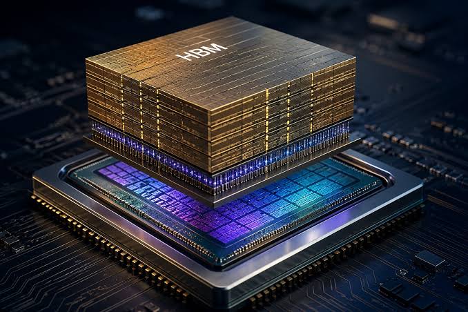
Samsung has outlined a three phase roadmap for future high bandwidth memory that would eventually move HBM from today’s 2.5D packaging into a true 3D structure stacked directly on top of an accelerator.
The long term design, called zHBM, is intended to reduce data movement, lower I/O power and free more silicon area for compute. Samsung is also expanding the role of the HBM base die, turning it from a relatively simple interface layer into a more active part of the memory system.
Samsung plans to make the HBM base die more intelligent
Current HBM consists of stacked DRAM core dies connected through TSVs to a base die. The base die handles functions such as data movement and connects the memory stack to the GPU, TPU or other accelerator through a PHY.
Samsung says bandwidth continues to rise with each HBM generation, but scaling is becoming harder because of limits around TSV density, I/O count, pin speed and PHY power.
The company says HBM4 already reaches more than 3TB/s per stack, while HBM4E is expected to move into the 4TB/s range. HBM5 is planned to push bandwidth even higher while also increasing capacity beyond 60GB per stack.
| Phase | Main focus | Key idea |
|---|---|---|
| Phase 1 | Reclaim XPU area | Smaller interfaces, thermal management and memory controller offload |
| Phase 2 | Add more functions | Telemetry, testing, memory extension and selective processing |
| Phase 3 | Full 3D integration | Stack zHBM directly on the accelerator |
Custom HBM moves more logic into the base die
Samsung’s first step is custom HBM, where advanced logic processes are used to add SoC style functions to the base die.
The company says this can reduce the size of the conventional HBM PHY and replace it with a shorter die to die interface. That could improve energy efficiency while freeing space on the accelerator for additional compute resources.
Samsung is also considering moving the memory controller from the accelerator into the HBM base die.
Other ideas include SRAM based repair mechanisms, advanced reliability monitoring, on die testing and memory extension controllers that could connect additional LPDDR or HBM capacity.
Selective processing elements could also be placed inside the memory system to reduce how much data needs to travel between memory and compute.
zHBM removes the 2.5D interposer
The third phase is the most significant.
Samsung’s zHBM concept would vertically stack HBM on top of the XPU instead of placing the memory beside it on a 2.5D interposer.
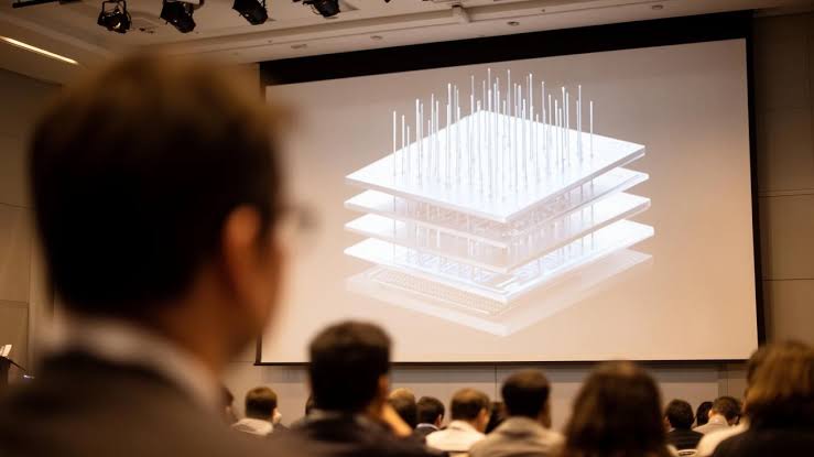
The design uses distributed I/O connections to shorten data paths and reduce the need for conventional SerDes links.
Samsung claims the approach could deliver around 230% more DRAM bandwidth and roughly 70% better power efficiency compared with a standard HBM4E configuration. It also estimates savings of up to 100W per DRAM module, potentially giving about 8.3% more power budget back to the accelerator.
Those figures are Samsung’s own projections and will need validation in production hardware.
Advanced bonding will be required
Samsung says zHBM will depend on advanced packaging technologies such as wafer on wafer bonding and Hybrid Cube Bonding.
These methods are intended to provide the very high I/O density needed to create a tightly integrated memory and compute structure.
The company’s broader target is around 0.5 pJ per bit for I/O power, along with more than twice the bandwidth of conventional designs and greater thermal headroom for the GPU or other accelerator.
If Samsung can move this roadmap into production, future HBM may become much more than stacked memory. The base die could increasingly handle control, repair, telemetry and selected compute functions, while zHBM would eventually place memory directly above the processor to reduce the distance data has to travel.

Discussion (0)
Be the first to comment.