

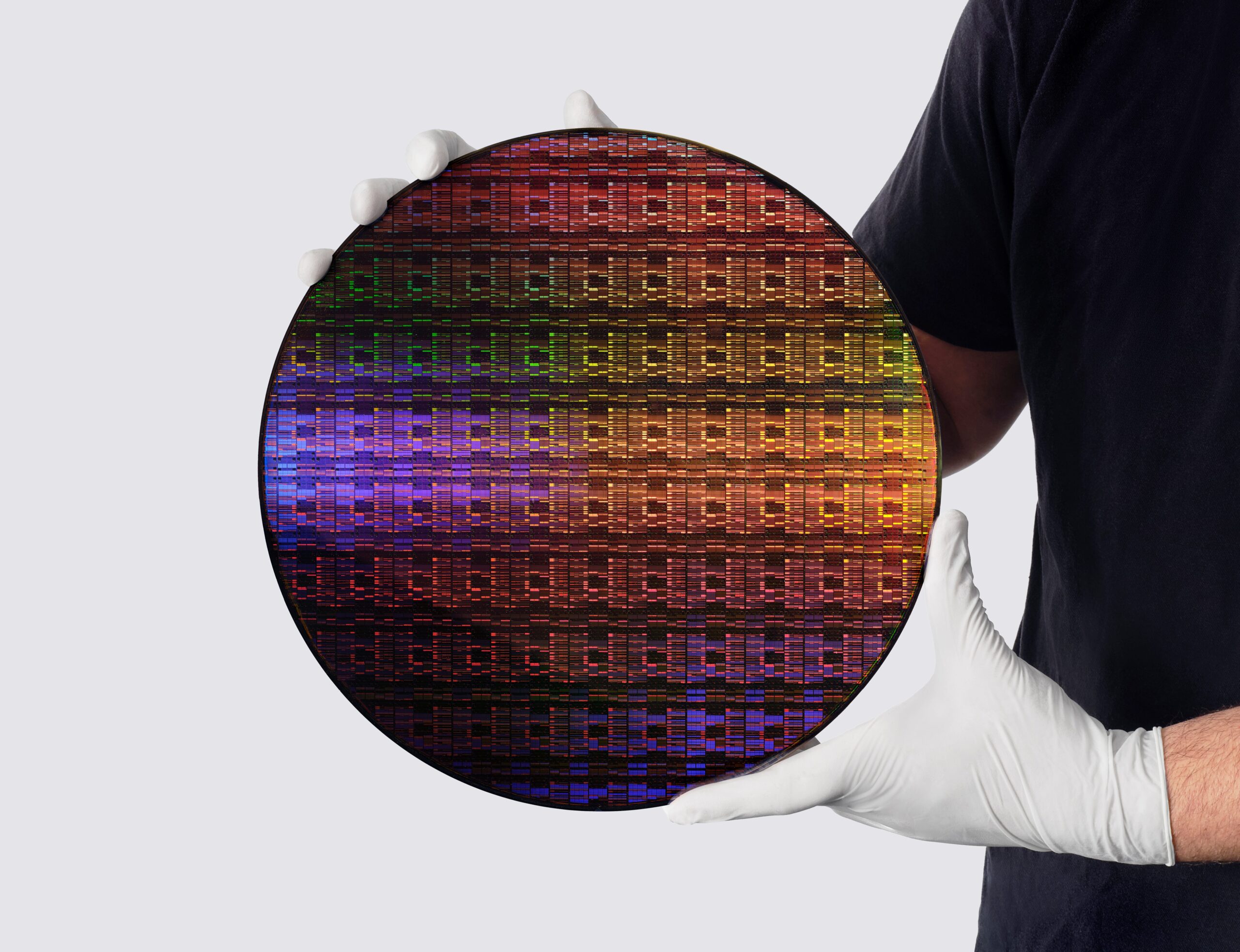
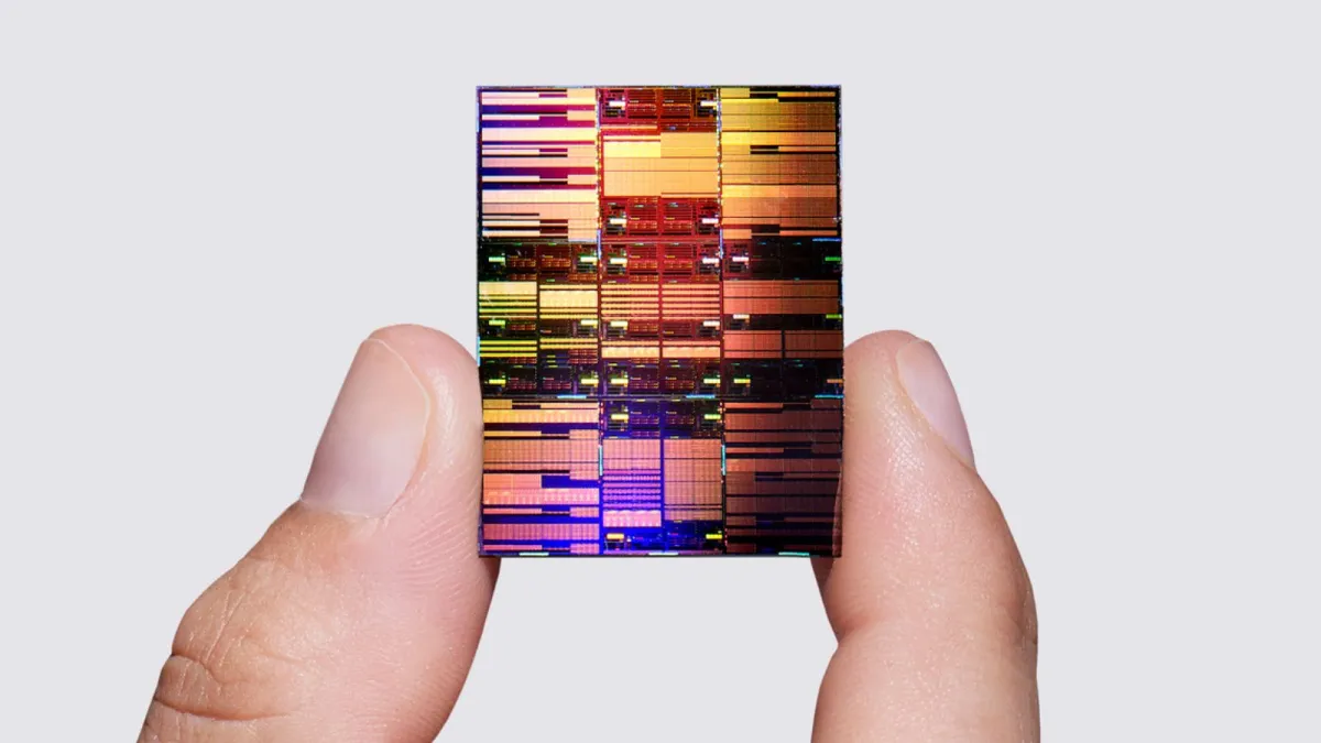
IBM has unveiled a new 0.7nm class chip technology that could reshape how future processors are built. The company says its Nanostack design can place nearly 100 billion transistors on a chip roughly the size of a fingernail, while offering up to 50% higher performance or 70% better energy efficiency than its earlier 2nm research technology.
The announcement is important because chipmakers are reaching the limits of traditional transistor shrinking. Modern node names such as 2nm, 3nm, and 5nm no longer describe one exact physical measurement, but they still represent new generations of manufacturing technology. IBM’s 0.7nm work is therefore less about a literal transistor width and more about a new way to increase density.
Instead of placing transistors side by side on a flat surface, IBM’s Nanostack approach builds them vertically. That could help the industry continue improving processor performance and efficiency even as conventional scaling becomes harder at atomic levels.
IBM Is Moving Beyond Flat Transistor Layouts
Today’s most advanced processors use gate all around transistor designs, where transistor channels are surrounded by the gate for better control and lower leakage. IBM’s Nanostack concept builds on that direction by stacking complementary transistor structures on top of each other.
This three dimensional approach reduces the amount of horizontal space needed for each transistor pair. In simple terms, IBM is trying to increase density by building upward instead of relying only on making every part smaller.
| IBM Nanostack claim | Reported improvement |
|---|---|
| Process class | 0.7nm or 7 angstroms |
| Transistor count | Nearly 100 billion |
| Density compared with IBM 2nm | Nearly double |
| Performance gain | Up to 50% |
| Energy efficiency gain | Up to 70% |
| SRAM scaling improvement | Around 40% |
| Potential production target | Within five years |
IBM also says the architecture allows different transistor layers to use different materials or tuning methods. That could help engineers optimize one part of the stack for speed and another for lower power use.
SRAM Gains Could Matter for AI Processors
One of the more notable claims is a 40% improvement in SRAM scaling. SRAM is used for processor cache, which stores data close to the CPU or GPU cores for faster access.
This matters for AI processors, data centre chips, graphics hardware, and high performance computing systems. These workloads depend heavily on moving data quickly and efficiently. Improving cache density can reduce bottlenecks while helping processors use less power.
IBM has demonstrated functional CMOS inverter operation with the new architecture, showing that the technology can perform basic computation rather than existing only as a theoretical design.
Manufacturing Remains the Biggest Challenge
The technology is still at a research stage, and moving from a test chip to high volume production will be difficult. Stacking transistor layers requires extremely accurate alignment, reliable bonding, effective heat management, and high manufacturing yields.
Those challenges could make the process expensive, especially at first. IBM has said it believes Nanostack technology could enter production within five years, but it has not announced a manufacturing partner.
The company has a history of developing advanced chip research before other companies turn it into commercial products. Its earlier 2nm work was later licensed for manufacturing efforts in Japan.
IBM’s 0.7nm announcement does not mean consumer PCs will soon use sub 1nm processors. However, it offers a possible path forward for an industry that can no longer depend on simply shrinking flat transistors every generation. The future of chip design may increasingly depend on stacking components in three dimensions.


Discussion (0)
Be the first to comment.