

IBM has unveiled new 0.7nm chip manufacturing research built around a technology it calls Nanostack. The company says the approach could greatly increase transistor density by stacking transistor structures vertically, rather than relying only on making them smaller across a flat chip surface.
The announcement places IBM among the first companies to publicly discuss semiconductor technology below the 1nm generation. While the 0.7nm label does not describe one exact physical feature on the chip, IBM says the technology represents a major new manufacturing approach that could improve performance, power efficiency, and chip density.
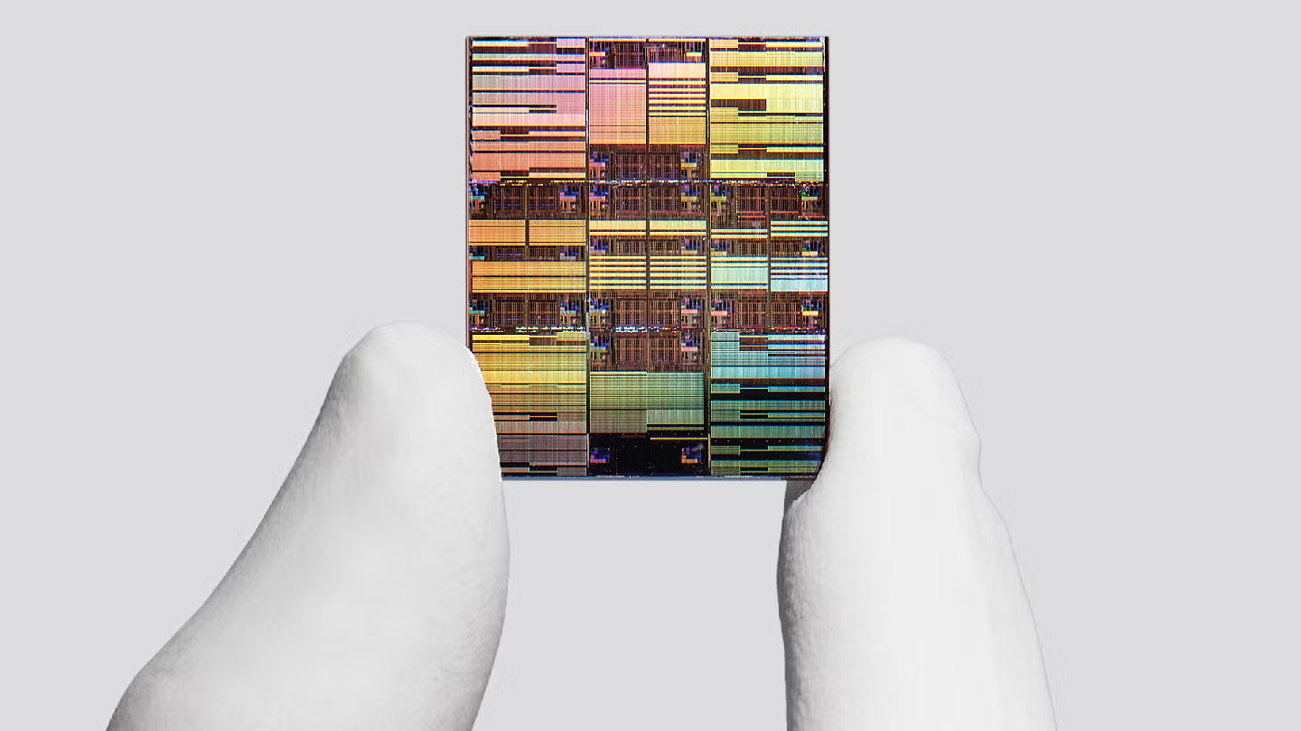
IBM claims its new process can fit up to 100 billion transistors into an area roughly the size of a fingernail. That could make future chips more capable without requiring much larger dies, an important goal as demand grows for AI processors, high performance computing hardware, and more efficient mobile devices.
Nanostack Builds on IBM’s Earlier Nanosheet Work
IBM previously introduced a 2nm process concept in 2021 that used nanosheet transistor technology. Nanosheet transistors are designed to give chipmakers more control over power use and performance than older FinFET designs.
Nanostack takes that idea further by arranging and staggering transistor structures vertically. The 3D design allows more components to be placed in the same area, helping increase density without depending entirely on traditional shrinking methods.
IBM says the new technology uses wafer bonding to create multilayer transistor structures. This requires extremely precise alignment between the bonded layers, making the manufacturing process more complex but potentially more capable.
| IBM Manufacturing Research | Main Technology | Claimed Benefit |
|---|---|---|
| 2nm process concept | Nanosheet transistors | Higher performance or lower power use |
| 0.7nm Nanostack concept | Vertically stacked transistor structures | Greater density and improved efficiency |
| Wafer bonding | Multi layer chip construction | Enables 3D transistor integration |
The company describes Nanostack as an evolution beyond nanosheet technology, with the goal of creating more advanced processors through vertical integration.
IBM Claims Major Improvements Over Its 2nm Technology
IBM says its 0.7nm technology could provide up to 50% higher performance or 70% better power efficiency compared with its earlier 2nm chip technology. These figures are based on research projections and should not be treated as real world product results yet.
The company also believes the technology could have a major impact on AI hardware. IBM estimates that future AI chips based on the process could reach up to 9,000 trillion operations per second, compared with around 4,500 TOPS for current high performance systems.

That kind of increase could reduce the time needed to train some AI models. IBM suggests tasks that currently take months could eventually be completed in weeks, though actual results would depend on chip design, memory, software, cooling, and the type of AI workload.
Smaller Node Labels Do Not Tell the Full Story
The 0.7nm name sounds like a direct measurement, but modern chip process labels are no longer as simple as they once were. A node name now usually describes a broader generation of technology, including transistor architecture, density, power efficiency, packaging, and manufacturing techniques.
IBM has acknowledged that its 7 angstrom label does not refer directly to the width of a specific printed feature. Instead, it represents the new manufacturing generation built around Nanostack.
That does not make the research less important. The key development is the shift toward stacking transistors and using wafer bonding to build denser chips. As traditional scaling becomes harder and more expensive, companies will increasingly depend on 3D chip designs, advanced packaging, and new materials to improve performance.
IBM’s 0.7nm research is still far from appearing in consumer processors. But it offers a look at how future chip manufacturing may move beyond simple shrinking and toward more complex vertical designs.


Discussion (0)
Be the first to comment.