

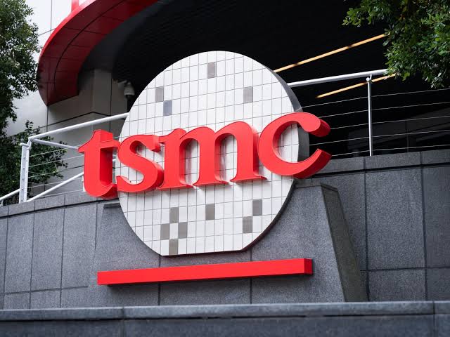
TSMC, Intel, and several major semiconductor companies are investing heavily in glass substrates and panel-level packaging as AI chips become larger, hotter, and more difficult to manufacture using traditional packaging methods.
The shift is being driven by AI data centres and high-performance computing systems that need bigger chip packages, faster communication between chiplets, more memory, and improved thermal control. Industry estimates suggest the market for fan-out panel-level packaging and glass substrates could grow from about $650 million in 2024 to more than $8 billion by 2030.
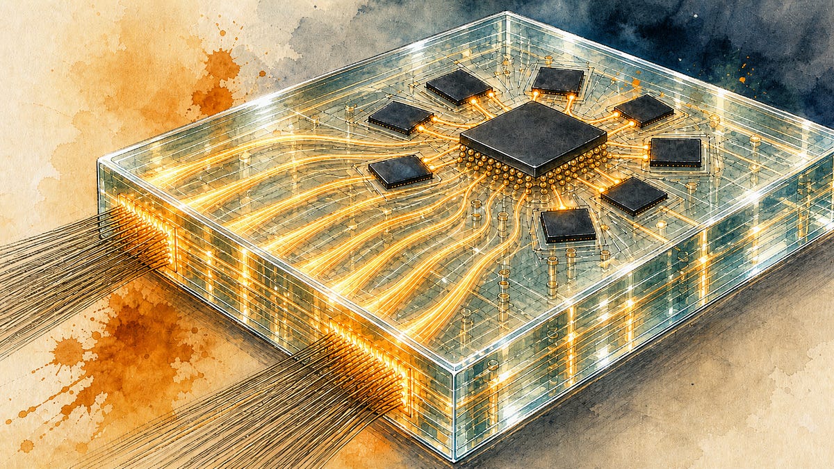
That growth would make advanced packaging one of the most important parts of the chip industry. Modern processors are no longer built around one large silicon die. They increasingly combine several compute chips, memory stacks, input and output dies, and specialised accelerators inside one package.
Glass Substrates Could Replace Traditional Organic Materials
Most advanced chip packages today use organic substrates to connect the processor, memory, and other components to a motherboard. These materials work well for current designs, but they become harder to manage as packages grow larger and more complex.
Glass substrates offer several potential advantages. They can provide better dimensional stability, reduced warping, higher interconnect density, and improved thermal characteristics. These benefits are important for AI processors that contain multiple chiplets and large stacks of high-bandwidth memory.
| Technology | Main benefit |
|---|---|
| Organic substrate | Common and widely used today |
| Glass substrate | Better stability and denser connections |
| Wafer-level packaging | Works well for smaller chip packages |
| Panel-level packaging | Supports larger packages and more dies |
| HBM memory packaging | Enables high bandwidth for AI workloads |
Glass also makes it easier to create larger package designs without some of the limitations found in conventional materials. That could be useful for future AI accelerators, data centre GPUs, networking chips, and high-performance CPUs.
Panel-Level Packaging Can Fit More Chips Into Each Production Run
Fan-out panel-level packaging uses large rectangular panels instead of round silicon wafers. This gives manufacturers more usable surface area and can reduce costs for large chip packages.
A larger panel can hold more compute dies, memory chips, and interposers during manufacturing. That is especially useful for AI hardware, where packages are becoming larger because of high-bandwidth memory and multi-chip designs.
The technology could also improve area efficiency. Traditional 300mm wafers are circular, which means some space is lost around the edges. Large panels can reduce that wasted space and improve the number of usable packages produced per manufacturing cycle.
TSMC is developing its Chip-on-Panel-on-Substrate approach, also known as CoPoS. The company is expected to first use traditional organic materials before moving toward glass core substrates later.
Intel Is Also Expanding Its Glass Packaging Plans
Intel has been one of the most vocal companies discussing glass substrates and panel-level packaging. The company has previously said that glass could help support the next generation of advanced chiplet designs.
Intel’s packaging work includes technologies designed to connect multiple chip dies inside one product. The company is also preparing facilities in the United States that could become important hubs for future glass substrate and panel-level packaging production.
Samsung Electro-Mechanics, ASE, PTI, and other companies are also investing in similar technologies. This means the industry is moving toward a broader packaging transition instead of relying on one company or one manufacturing method.
Asia Will Remain Central to Panel Packaging Growth
Taiwan, China, and Japan are expected to account for a large share of global panel-level packaging capacity by 2030. These regions already play major roles in semiconductor manufacturing, substrates, packaging, testing, and memory production.
TSMC’s large packaging investments in Taiwan will be especially important because companies such as Nvidia, AMD, Apple, and Google rely heavily on its manufacturing capacity.
However, the technology still faces major challenges. Companies need common panel size standards, reliable through-glass via connections, stable production yields, and proven long-term manufacturing processes.
Advanced Packaging Is Becoming as Important as Chip Design
For years, chip performance mainly depended on making transistors smaller. That remains important, but it is no longer enough on its own.
AI processors now need huge memory bandwidth, more chiplets, better cooling, and high-speed communication between components. Advanced packaging is becoming the way companies solve those problems.
Glass substrates and panel-level packaging may not reach mainstream use immediately, but they are likely to play a major role in the next generation of AI and high-performance computing hardware.

Discussion (0)
Be the first to comment.