

Nvidia’s future Feynman AI chip could become one of the first major products to use TSMC’s next generation CoPoS packaging technology, according to analyst Ming Chi Kuo. The new packaging method is expected to enter mass production in the second half of 2028 and is designed to support much larger AI chip packages than today’s CoWoS technology can handle.
The report matters because advanced AI chips are no longer limited only by transistor scaling. Packaging has become just as important. Nvidia, AMD, Broadcom, Google, Amazon, and other AI chip developers need more room for compute dies, memory stacks, interconnects, and power delivery. Current CoWoS packaging has helped make today’s AI accelerators possible, but its size limits are becoming harder to ignore.
TSMC’s CoPoS, short for chip on panel on substrate, is meant to solve that problem by moving beyond the constraints of traditional wafer based interposer packaging.
CoPoS is being built for larger AI chip packages
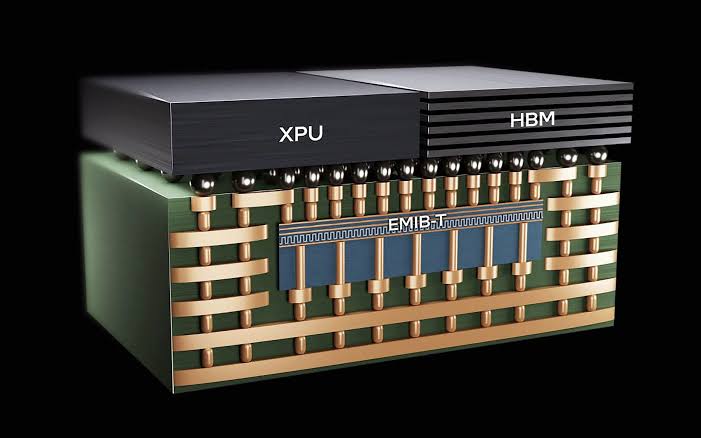
Today’s high end AI accelerators often use CoWoS packaging, where a silicon interposer connects the GPU die, HBM memory, and other chip components. This provides fast communication between parts of the package, which is critical for AI training and inference performance.
The limitation is size. CoWoS relies on lithography tools to make the interposer, and those tools are restricted by reticle size. As AI chips grow larger, companies need packages that exceed what current CoWoS can economically support.
| Packaging technology | Main purpose |
|---|---|
| CoWoS | Current advanced packaging for GPUs and HBM |
| CoPoS | Next generation packaging for ultra large AI chips |
| Main advantage of CoPoS | Supports larger package sizes beyond CoWoS limits |
| Expected mass production | Second half of 2028 |
| Possible early adopter | Nvidia Feynman AI chip |
| Key material detail | Glass core substrate with ABF layers |
CoPoS avoids some of the CoWoS size limits by using a panel based approach instead of relying on the same interposer structure. That could allow TSMC to build much larger packages for future AI accelerators.
Nvidia Feynman may need packaging beyond today’s CoWoS
Nvidia’s Feynman AI chip is expected to arrive after the company’s current and near future AI platforms. If the chip continues the industry trend toward larger packages, more memory, and more compute, it may require packaging that stretches beyond current CoWoS capacity.
That is why Feynman is being linked to both TSMC’s CoPoS and, in some supply chain reports, Intel’s EMIB T technology. Nvidia is likely studying multiple packaging paths because future AI chips will need more advanced interconnect and larger assembly areas.
This does not mean Nvidia has fully moved away from TSMC. TSMC remains the dominant foundry and packaging partner for leading AI chips. But the pressure on packaging capacity and package size is now large enough that Nvidia may evaluate every viable option.
CoPoS will use a glass based substrate structure
Kuo clarified that CoPoS should not be confused with a glass interposer design. According to the analyst, CoPoS uses glass first as a temporary carrier during assembly and then in the final substrate structure.
The final substrate is described as a glass core placed between layers of ABF, or Ajinomoto Buildup Film. The chip components are attached to the ABF layer, not to a glass interposer.
This distinction is important because glass is becoming a major topic in advanced packaging. It can help with rigidity, flatness, and larger package support, but using it in production at scale is still a major manufacturing challenge.
TSMC is trying to protect its AI packaging lead
TSMC has already become a central supplier for AI chip manufacturing, but demand has stretched its CoWoS capacity. If CoPoS arrives in 2028, it could help TSMC stay ahead as AI chip packages grow beyond current limits.
The timing also matters. AI chip makers are racing to increase performance with more compute, more HBM, and larger package level designs. If TSMC cannot offer a large enough packaging platform, customers may look at Intel, Samsung, or other advanced packaging suppliers.
CoPoS gives TSMC a clear answer for the next phase of AI hardware. It is not just about making chips smaller. It is about making complete AI packages bigger, faster, and more efficient.
Advanced packaging is becoming the new AI chip battlefield
The Nvidia Feynman and TSMC CoPoS report shows where the AI hardware race is heading. Chipmakers are still improving architectures and process nodes, but packaging is now one of the main limits on progress.
More powerful AI chips need more HBM stacks, wider interconnects, larger substrates, and stronger power delivery. That creates a packaging problem before it becomes a software or model problem.
For Nvidia, CoPoS could provide the room needed for a much larger post Rubin AI chip. For TSMC, it could extend the company’s dominance in AI chip manufacturing beyond the CoWoS era.
If CoPoS reaches mass production in 2028 as expected, it may become one of the key technologies behind the next generation of AI accelerators. The Feynman chip could be the first major test of whether TSMC can scale advanced packaging fast enough for the next wave of AI demand.
Discussion (0)
Be the first to comment.