

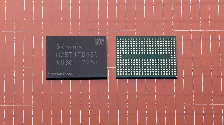
SK Hynix is reportedly preparing to begin mass production of its 375 layer NAND flash by the end of 2026, marking its next major step in the race against Samsung for higher density storage. The company has completed verification of the new NAND design and is expected to move production into existing fabs after converting them for the newer process.
The move matters because NAND makers are trying to increase storage capacity by stacking more layers inside memory chips. More layers can help improve density, reduce cost per bit over time, and support larger SSDs for PCs, servers, phones, and AI infrastructure.
SK Hynix had internally treated this generation as a 400 layer class product, but the final design reportedly lands at 375 layers. The reduction appears to be tied to the technical difficulty of stacking so many layers while maintaining reliable signal transmission and manufacturing yields.
SK Hynix is moving from 321 layer NAND to 375 layer NAND
SK Hynix is currently producing 321 layer V9 NAND flash, and the next step will be the 375 layer design. The new product is expected to use converted production lines inside existing fabs rather than an entirely new factory buildout.
That approach can help reduce the time and cost needed to move into production, but it still requires process changes, equipment adjustments, and validation.
| NAND generation | Reported status |
|---|---|
| 321 layer NAND | Currently in production |
| 375 layer NAND | Verified and expected for mass production by late 2026 |
| 480 layer NAND | Planned for a later generation |
| 604 layer NAND | Part of the longer term roadmap |
| 400 layer class label | Internal class name reportedly revised to 375 layers |
The 375 layer product should help SK Hynix stay competitive as Samsung pushes toward 400 layer and higher V NAND products.
Tungsten is becoming a problem for higher layer NAND
The bigger technical shift is material related. SK Hynix is reportedly preparing to move away from tungsten in future NAND designs because the material becomes harder to use as wiring gets narrower and layer counts increase.

Tungsten has been widely used in semiconductor processes, but it can create signal transmission problems as resistance becomes harder to manage at smaller dimensions. As NAND stacks grow taller, those limitations become more difficult to work around.
That is why future SK Hynix products, including 480 layer and 604 layer NAND, are expected to require a move toward molybdenum. Samsung is already using molybdenum in some NAND products, giving it an early advantage in this material transition.
Molybdenum demand could rise quickly
The shift from tungsten to molybdenum could reshape part of the semiconductor materials supply chain. As NAND makers adopt the new material for future high layer products, demand is expected to rise sharply.
Samsung reportedly bought around 4 tons of molybdenum last year and has already purchased around 10 tons this year. SK Hynix is expected to use around 4 tons as it prepares its own transition.
| Year | Expected molybdenum demand |
|---|---|
| 2027 | Around 25 tons |
| 2028 | Around 40 tons |
| 2029 | Around 60 tons |
| 2030 | Around 80 tons |
This matters because memory makers are already dealing with material cost pressure, AI driven demand, and tighter supply chains. A major material shift could add more complexity before it eventually improves production efficiency.
Samsung and SK Hynix are racing toward higher density storage
Samsung and SK Hynix are both pushing NAND layer counts higher because storage demand continues to grow. AI servers, high capacity SSDs, smartphones, laptops, gaming PCs, and enterprise storage systems all need more NAND.
Samsung is aiming beyond 400 layers and is also exploring dual stack approaches that could eventually scale much higher. SK Hynix’s roadmap points to 480 layer and 604 layer NAND after the 375 layer generation.
The challenge is that higher layer counts are not only about stacking more cells. Manufacturers must keep performance, endurance, power use, signal integrity, and yields under control. A chip that is too difficult or expensive to manufacture will not help much, even if the layer count sounds impressive.
The NAND race could affect SSD pricing and capacity
For consumers, these developments may eventually lead to larger SSDs and better storage density. In the short term, however, the transition could add cost pressure because manufacturers need new materials, converted production lines, and refined processes.
AI demand is also increasing pressure on storage and memory markets. Data centers need more NAND for fast storage, while HBM and DRAM demand are already reshaping supplier priorities.
SK Hynix’s 375 layer NAND is an important step, but the bigger story is the industry’s move beyond tungsten. As NAND makers push past 400 layers, material limits are becoming just as important as manufacturing skill.
If SK Hynix can move smoothly from 375 layer NAND to its future 480 layer and 604 layer designs, it will remain a major competitor to Samsung in high density storage. But the next phase of NAND progress will depend not only on stacking more layers, but also on solving the material problems that come with going taller.


Discussion (0)
Be the first to comment.