




Intel’s work on glass core substrates is moving closer to real hardware, with early prototypes shown at the Optical Fiber Communication Conference 2026. The prototypes included co packaged optics, giving an early look at how advanced AI and HPC chips could be built near the end of this decade.
The prototypes were spotted by Dr. Ian Cutress of More Than Moore. They are described as mockups, so they should not be treated as finished commercial products. Still, they show the direction chip packaging is heading as AI systems demand more bandwidth, more chiplets, and better power efficiency.
Glass substrates could help chip makers fit more chiplets and optical links into one package
Glass core substrates are being explored as an alternative to today’s organic substrates. The industry is facing substrate supply pressure because of the AI hardware boom, and prices have already been rising at major suppliers. That has made advanced packaging a more important part of future chip design.
The mockup shown at OFC 2026 included compute chiplets, DRAM chiplets, smaller supporting chiplets, and eight yellow co packaged optical interfaces placed around the edge of the glass substrate. These optical interfaces are important because they can convert electrical signals into light on the package itself, reducing the need to rely only on copper for data transfer.
| Area | Why it matters |
|---|---|
| Glass core substrate | Could replace some organic substrates in advanced chips |
| Co packaged optics | Helps move data using optical links instead of only copper |
| AI and HPC chips | Need higher bandwidth and more efficient data movement |
| Expected rollout | Around 2029 to 2030 |
| Claimed benefit | Up to 10 times interconnect density |
| Industry pressure | AI demand is increasing substrate and packaging constraints |
Intel has already said it is working on glass substrates to replace organic packages in future chip designs. Partners such as Amkor have also pointed to readiness within about three years, which suggests the first broader rollout could happen around 2029 or 2030.
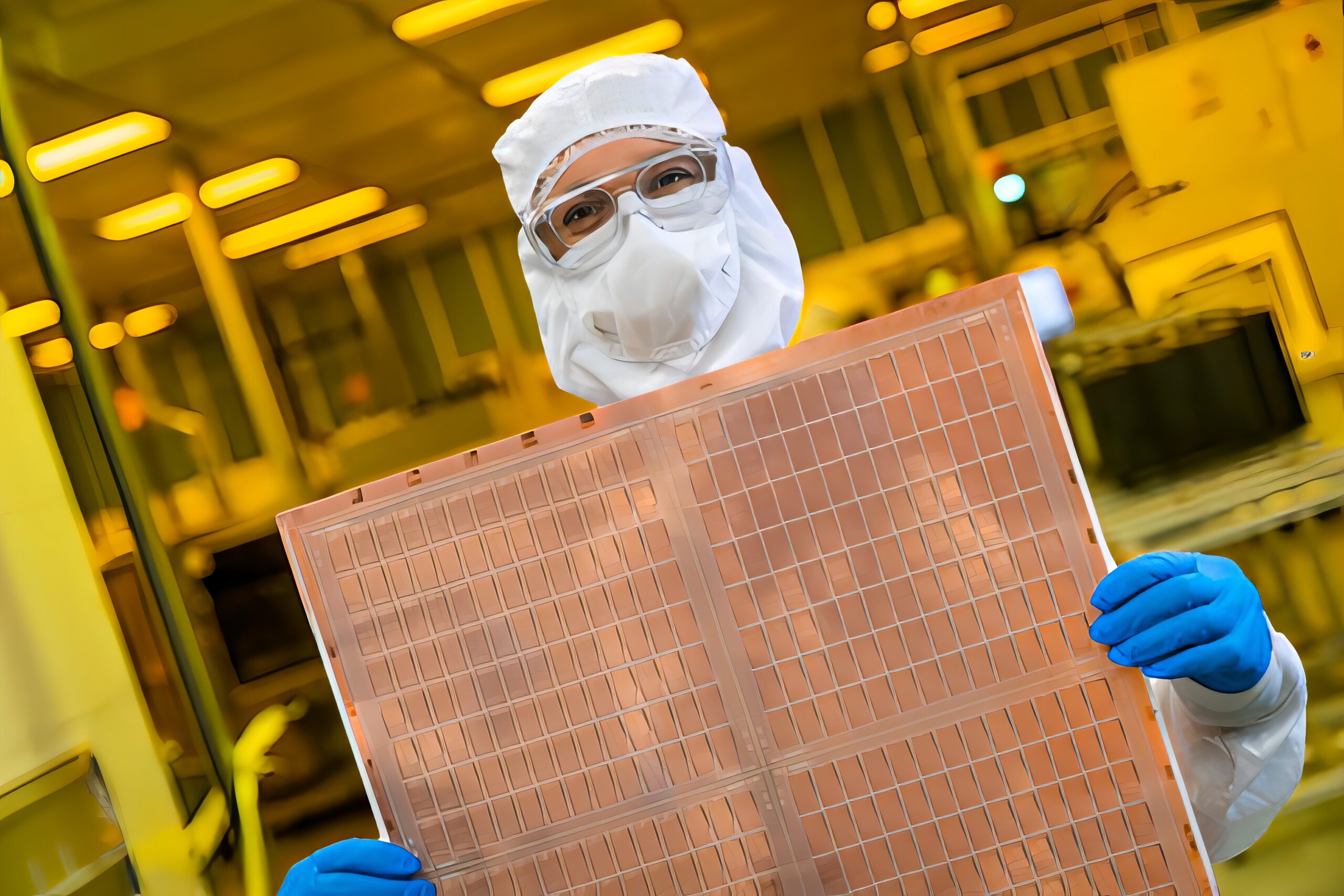
The main advantage is density. Glass substrates are expected to support much higher interconnect density, allow more chiplets in one package, and work well with optical interfaces such as co packaged optics. They may also improve yields because rectangular glass panels can be used instead of traditional round wafers.
For Intel, the technology could become important to its foundry ambitions. If glass substrates deliver the promised gains, they could help Intel compete for advanced AI packaging work as data center chips become larger, denser, and more dependent on high speed interconnects.
Discussion (0)
Be the first to comment.