



Fujitsu is preparing its next generation Monaka processor for production shipments in 2027, with a design that combines a 144 core Arm CPU built on a 2nm process with separate 5nm SRAM and I/O dies connected through advanced 3D packaging.
Monaka is being developed as the successor to Fujitsu's A64FX processor, which powered Japan's Fugaku supercomputer. The new chip targets AI and high performance computing workloads with Arm v9.3 A architecture, SVE2 support, low voltage operation and confidential computing capabilities.
The chip will be offered in two main versions. A high performance model runs at 2.9 GHz with a 500W TDP, while a more efficient version operates at 2.1 GHz with a 350W TDP.
| Monaka specification | High performance SKU | High efficiency SKU |
|---|---|---|
| CPU cores | 144 | 144 |
| Base frequency | 2.9 GHz | 2.1 GHz |
| TDP | 500W | 350W |
| DGEMM performance | 6013 GFLOPs | 4355 GFLOPs |
| INT8 performance | 96.2 TOPS | 69.7 TOPS |
| Cooling | Liquid | Air |
3D chiplet design separates compute from cache and I/O
Monaka uses a disaggregated architecture rather than putting every major component onto one large 2nm die.
The main compute chiplet uses TSMC's N2P process, while SRAM and I/O functions are moved to separate 5nm dies. The SRAM die sits underneath the compute die and contains the last level cache, with hybrid bonding providing a short connection between the two layers. The I/O portion connects through a silicon interposer.
Fujitsu says this design reduces the required 2nm silicon area by around 30 percent. That can help balance manufacturing cost, power consumption and performance because only the parts that benefit most from the newest process need to use it.
The hottest compute die is positioned on top to shorten the thermal path toward the cooler. Fujitsu is also using per core voltage and frequency control through integrated LDO circuitry.
Each Monaka core measures approximately 1.47 mm².
Monaka supports PCIe 6.0, CXL 3.0 and 12 channel DDR5
The platform includes substantial memory and expansion capability.
Each processor supports 96 PCIe 6.0 lanes with CXL 3.0 and 12 channel DDR5 memory rated at more than 8000 MT/s. A dual socket system can provide 288 CPU cores in a single node.
Fujitsu is also supporting several NUMA configurations. The processor can operate as eight 18 core NUMA nodes, four 36 core nodes or a single 144 core node depending on software and workload requirements.
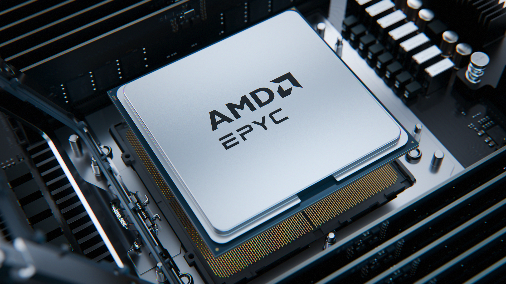
The custom core design includes SVE2 with two 256 bit execution units and two 256 bit load and store units. Support for formats including FP8 and INT8MM is intended to improve AI inference capability.
Fujitsu claims Monaka can provide up to twice the AI performance of its previous platform while reducing total cost of ownership by more than 50 percent through low voltage operation. Those figures are company targets rather than independent benchmark results.
Monaka X is planned for 2029
Fujitsu says Monaka is already sampling, with production shipments planned for 2027.
The company is also working on Monaka X for a targeted 2029 release. That processor is expected to add SME2 support for AI workloads and NVIDIA NVLink Fusion connectivity. Monaka X has also been selected for Japan's FugakuNext supercomputer project.
The roadmap shows Fujitsu continuing to combine Arm based CPU development with advanced packaging rather than relying on a single monolithic die. For large AI and HPC systems, that approach could give the company more flexibility in how it scales compute, cache, memory and interconnect performance across future generations.
Discussion (0)
Be the first to comment.