

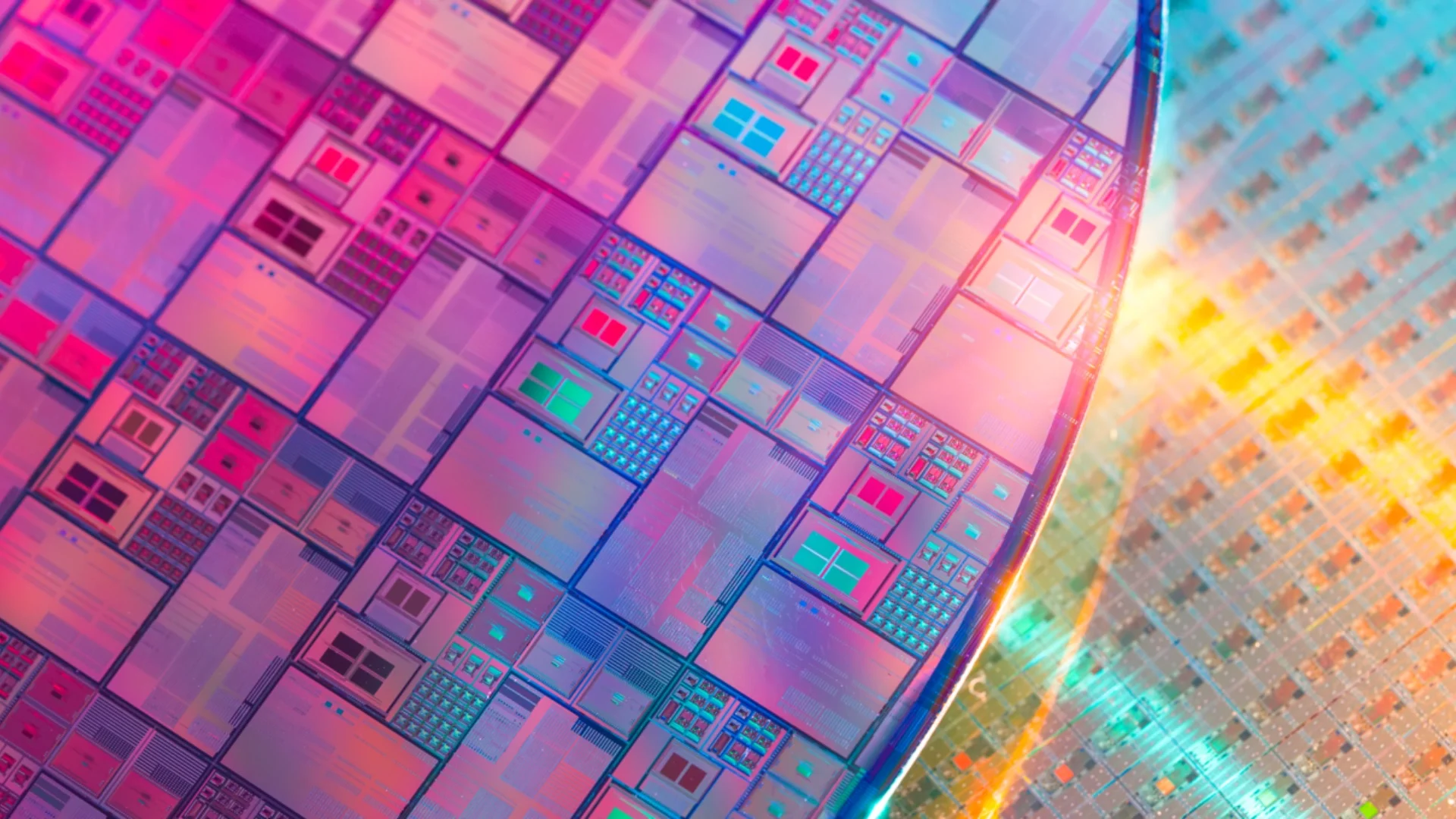
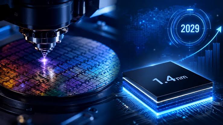
Samsung is reportedly preparing to restart development of its 1.4nm manufacturing technology, with mass production now expected in 2029. The move would put Samsung back into the race for the next major generation of advanced semiconductor production, where Intel and TSMC are also developing their own 1.4nm-class processes.
Samsung had previously planned to bring its SF1.4 node into mass production earlier, but the company reportedly shifted attention toward improving its 2nm technology first. That decision appears to have been based on the need to strengthen production yields, improve manufacturing reliability, and secure more customer confidence before moving to a more difficult node.
The company is now said to be pushing forward again with SF1.4, which could become a key part of Samsung Foundry’s long-term strategy.
Samsung Focused on 2nm Before Restarting 1.4nm Plans
Samsung’s 1.4nm technology was originally expected to reach mass production around 2027. However, the company reportedly delayed that target to concentrate on its SF2 and SF2P processes.
Those 2nm nodes are important because they are closer to commercial readiness and could help Samsung compete more directly with TSMC and Intel in the near term. Advanced process development is expensive, and companies must balance the need to move forward with the need to make each generation profitable and reliable.
Samsung’s reported decision to restart its 1.4nm plans suggests that the company believes it has made enough progress with 2nm manufacturing to begin preparing for the next step.
| Process technology | Reported focus | Expected timing |
|---|---|---|
| Samsung SF2 | Main 2nm production node | Near-term focus |
| Samsung SF2P | Improved 2nm derivative | Near-term focus |
| Samsung SF1.4 | Next-generation advanced node | Mass production targeted for 2029 |
| Intel 14A | Advanced foundry process | Expected before Samsung SF1.4 |
| TSMC A14 | Advanced 1.4nm-class node | Expected before Samsung SF1.4 |
High-NA EUV Could Give Samsung a Technology Advantage
Samsung is expected to use high numerical aperture EUV lithography equipment for its future 1.4nm process. These machines are designed to create smaller and more detailed chip patterns than earlier EUV tools.
High-NA EUV is one of the biggest technical changes coming to semiconductor manufacturing. It could help chipmakers improve transistor density and reduce the number of complicated manufacturing steps required for advanced nodes.
Samsung has reportedly received high-NA EUV equipment for its advanced semiconductor research facility. That could give the company a head start in learning how to use the technology before it reaches full production.
However, owning the equipment is only one part of the challenge. Samsung will still need to achieve strong yields, maintain stable production, and convince major chip designers that SF1.4 is ready for high-volume products.
Intel and TSMC Will Still Be Major Rivals
Samsung will face intense competition from Intel and TSMC. Intel is developing its 14A technology as part of its broader foundry expansion, while TSMC is working on its A14 node and continuing to lead the industry in advanced contract manufacturing.
Samsung may arrive later than both companies, but a 2029 launch could still be important if it offers clear advantages in performance, efficiency, cost, or manufacturing capacity.
The real battle will not be decided by node names alone. Customers will compare yields, power efficiency, performance, packaging options, supply reliability, and pricing before choosing a foundry partner.
Samsung’s return to the 1.4nm roadmap shows that the company is not stepping away from the advanced process race. The next few years will determine whether SF1.4 becomes a serious alternative to Intel 14A and TSMC A14, or remains another ambitious technology plan that struggles to reach large-scale production.

Discussion (0)
Be the first to comment.