



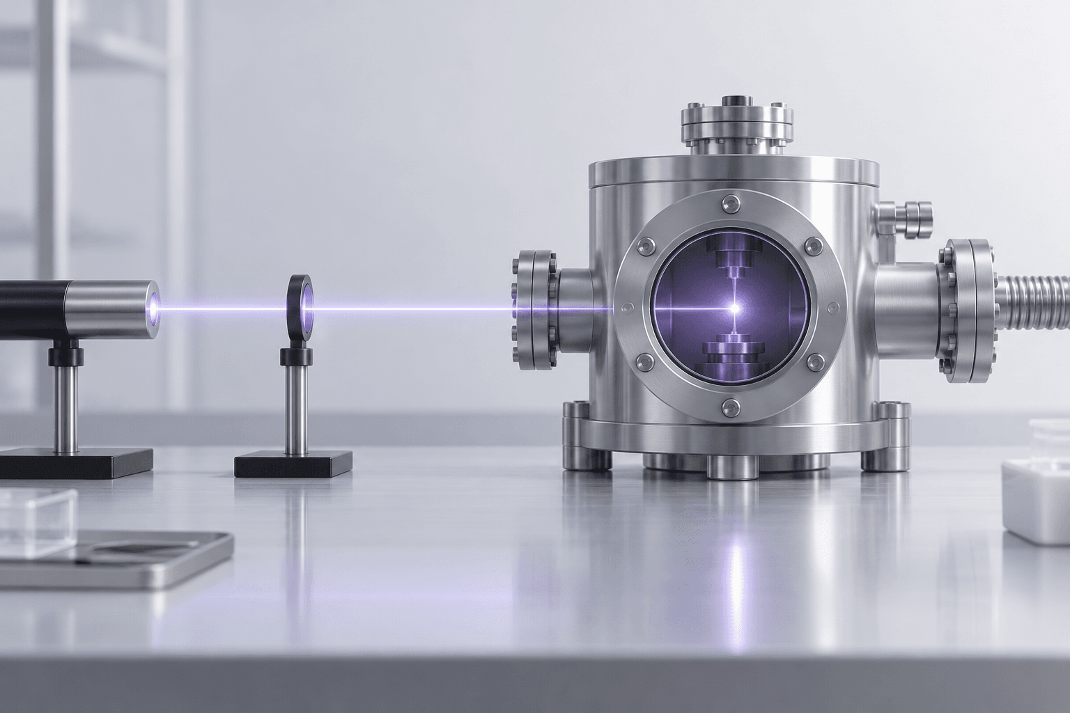
A Chinese technology startup has unveiled a prototype extreme ultraviolet light source designed for advanced semiconductor lithography, marking another step in China’s effort to reduce its dependence on foreign chipmaking equipment.
The prototype, called FlintNano LPP OXXO, was shown at the 26th China International Industry Fair in Shanghai. Its developer says around 90% of the system’s core components were sourced through domestic research and development.
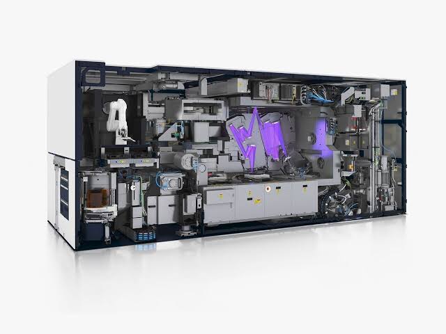
The light source is an important part of an EUV lithography machine, but it is only one component of a much larger system. Commercial EUV equipment also requires highly advanced optics, precision wafer stages, control systems and complex integration.
FlintNano Uses Laser Produced Plasma Technology
The prototype uses laser produced plasma, or LPP, technology.
This method fires a high power laser at a target to create plasma that emits EUV light. It is broadly the same technical approach used in existing commercial EUV systems.
The company disclosed several specifications for its prototype.
| Specification | FlintNano LPP OXXO |
|---|---|
| Driving laser output | 1,000W |
| Repetition rate | 1 to 20kHz |
| Conversion efficiency | Above 2% |
| EUV output | At least 15W |
| Continuous operation | More than 100 hours |
| Plasma size | 60μm |
| Plasma stability | 3% RMS |
| Energy stability | About 5% |
| Reported localization rate | About 90% |
The developer says the prototype has reached a level suitable for wafer exposure testing.
That represents progress, but it is still far removed from the requirements of high volume semiconductor manufacturing.
Commercial Production Is Still a Major Challenge
The startup estimates that another three to five years could be required before large scale commercial production becomes possible.
That timeline remains uncertain.
Building a functioning EUV light source does not mean China has completed a commercially viable EUV lithography platform. A complete machine requires multiple technologies that are difficult to develop and manufacture at the precision needed for leading edge semiconductor production.
These include ultra precision mirrors and optics, wafer positioning systems, vibration control, vacuum systems and the software required to synchronize hundreds of thousands of individual components.
The supplied information notes that current Chinese deep ultraviolet lithography systems still lag established international equipment, suggesting that developing a competitive EUV machine could take considerably longer than the startup’s three to five year estimate.
Some industry estimates have suggested that closing the broader equipment gap could take eight to ten years, while another semiconductor industry executive has previously suggested a period of roughly 15 years.
These longer estimates are not guarantees, but they illustrate the difference between demonstrating an individual component and producing a complete commercial lithography system.
EUV Machines Depend on a Large Supply Chain
Modern EUV lithography tools are extremely complex.
Existing commercial systems contain hundreds of thousands of components sourced from more than 800 suppliers.
A high power EUV light source is one of the most technically demanding parts of the platform, but other subsystems must achieve equally demanding levels of precision and reliability.
The challenge is also not limited to whether a machine can expose a wafer.
For semiconductor manufacturers, production equipment must operate continuously, maintain extremely tight tolerances, deliver high throughput and achieve economically viable yields across thousands of wafers.
Those manufacturing requirements are much harder to satisfy than demonstrating a laboratory prototype.
China Continues to Push for Domestic Lithography Technology
China has invested heavily in domestic semiconductor equipment as export restrictions limit access to advanced foreign technology.
Earlier reports have pointed to Chinese EUV prototype development and trial production efforts beginning as early as 2025.
The FlintNano demonstration adds another visible piece to that broader effort.
Its claimed 90% localization rate is also significant because China is trying to reduce reliance not only on complete lithography systems but also on imported subsystems and components.
However, the new light source does not yet represent a direct replacement for existing commercial EUV machines.
The more immediate milestone will be whether the prototype can move from wafer exposure testing to reliable, high power operation at the throughput and stability needed for semiconductor manufacturing.
For now, FlintNano shows that domestic EUV development is progressing, but a complete production ready lithography system remains a much larger engineering challenge than the light source alone.
Discussion (0)
Be the first to comment.