

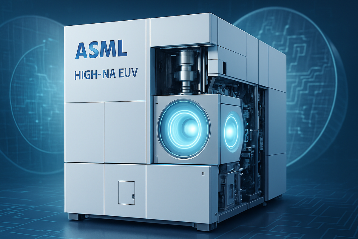
ASML is preparing the next stages of EUV lithography as AI demand pushes chip factories toward tighter capacity limits. The company’s High NA EUV systems are moving closer to high volume manufacturing, while its longer term Hyper NA plans are being positioned as the next step for advanced chips beyond the early 2030s.
EUV lithography is one of the most important bottlenecks in modern semiconductor production. Leading chip nodes below 7nm depend on EUV tools, and ASML remains the only company that supplies these machines at scale. As AI companies, cloud providers, and chip designers demand more advanced silicon, foundries need more EUV capacity and better tools to keep shrinking chip features.
That is why ASML’s roadmap matters. The company is not only trying to build more machines. It is also trying to make each generation of EUV more efficient by reducing the number of exposure and mask steps needed to produce advanced chips.
Why EUV capacity matters for AI chips
AI infrastructure depends on many layers, including power, packaging, networking, memory, and advanced logic. But none of those layers can scale without enough wafers from leading edge fabs.
The most advanced AI accelerators use cutting edge process nodes, and those nodes rely heavily on EUV lithography. If foundries cannot get enough EUV tool capacity, chip output becomes constrained even if demand from companies such as NVIDIA, Google, AMD, Apple, and hyperscalers keeps rising.
Foundries can improve uptime and utilization, but that only goes so far. There are only so many EUV systems available each year, and customers are competing for allocations.
| EUV generation | Main purpose |
|---|---|
| 0.33 NA EUV | Current low NA EUV used in leading production |
| 0.55 High NA EUV | Reduces multi patterning and supports smaller features |
| Hyper NA EUV | Planned future step beyond 0.75 NA for nodes past A7 |
| EXE platform | ASML’s high performance platform for High NA and future systems |
| Main benefit | Fewer mask steps, shorter cycle times, and better scaling |
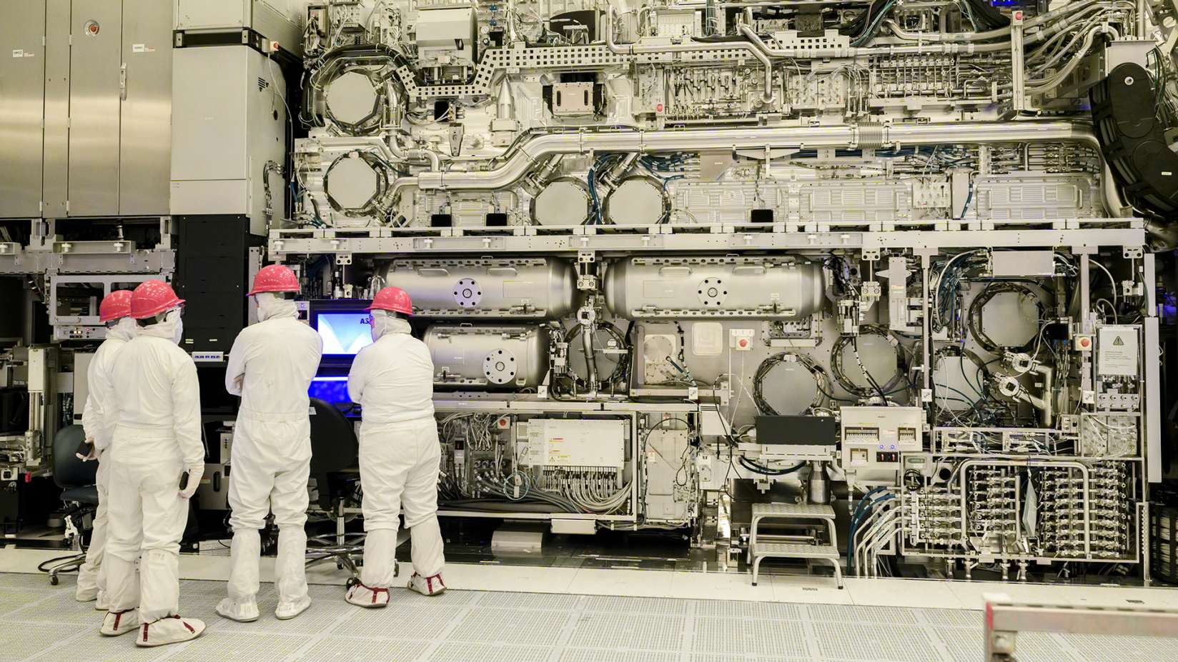
High NA EUV is getting closer to real production
ASML’s High NA journey has taken years, but it is now moving from early deployment toward broader production qualification. The first 0.55 NA system, the EXE:5000, shipped in the fourth quarter of 2023. The first wafer exposure followed in the third quarter of 2024.
The newer EXE:5200B was first delivered to customers in the fourth quarter of 2025. It can reach 175 wafers per hour, helped by the 1000W laser source ASML revealed in 2025. Earlier EXE:5000 systems were rated at 110 wafers per hour.
The progress is important because High NA can reduce the number of exposures required for advanced patterns. Intel has been one of the earliest and most aggressive adopters, and the company has indicated that moving from 0.33 NA to 0.55 NA can reduce certain exposure steps from three to one, with similar benefits in mask processing.
That matters for cost, cycle time, and complexity. The fewer times a wafer needs to pass through lithography and related steps, the easier it becomes to scale future nodes.
Hyper NA is ASML’s next long term EUV step
ASML is already looking beyond High NA. The company has introduced Hyper NA EUV as the next major stage, defined as numerical aperture above 0.75.
Hyper NA is aimed at future nodes beyond A7, with that class of manufacturing expected around 2033. ASML’s view is that another numerical aperture increase will likely be needed in the second half of the 2030s to keep single exposure patterning practical.
The good news is that Hyper NA is not expected to require drastically larger optics than High NA. That gives ASML a path to reuse the high performance EXE platform introduced with High NA systems.
That continuity could help control some complexity, even if Hyper NA machines are expected to be extremely expensive when they first arrive.
Higher NA can reduce energy use despite rising chip complexity
One of the major advantages of moving to higher NA EUV is not only smaller features. It can also reduce the number of mask steps needed in production.
That can lower cycle time and reduce energy per wafer, even as chip designs become more complex. This is becoming increasingly important as AI chips push fabs, power systems, and supply chains harder.
High NA and Hyper NA tools will cost more than older EUV systems, but ASML’s argument is that the total manufacturing flow can become more efficient as multi patterning is reduced.
For foundries, that tradeoff may become necessary. A more expensive lithography tool can still make sense if it reduces process steps, improves yield, and helps keep advanced nodes economically viable.
ASML remains central to the future of advanced chips
The AI boom has created new bottlenecks across the semiconductor industry, from HBM memory to advanced packaging and power delivery. But EUV remains one of the most important constraints because it sits at the center of leading edge chip manufacturing.
ASML’s High NA systems are now approaching the stage where they can support high volume production, while Hyper NA is being planned as the longer term bridge into the next decade of scaling.
The timeline is still long, and each new EUV generation will bring cost, engineering, and adoption challenges. But the direction is clear. If the industry wants smaller, denser, and more power efficient chips for the hyperscale AI era, EUV has to keep advancing.
For ASML, that makes High NA and Hyper NA more than roadmap upgrades. They are the tools that could decide how far advanced semiconductor scaling can continue.

Discussion (0)
Be the first to comment.