


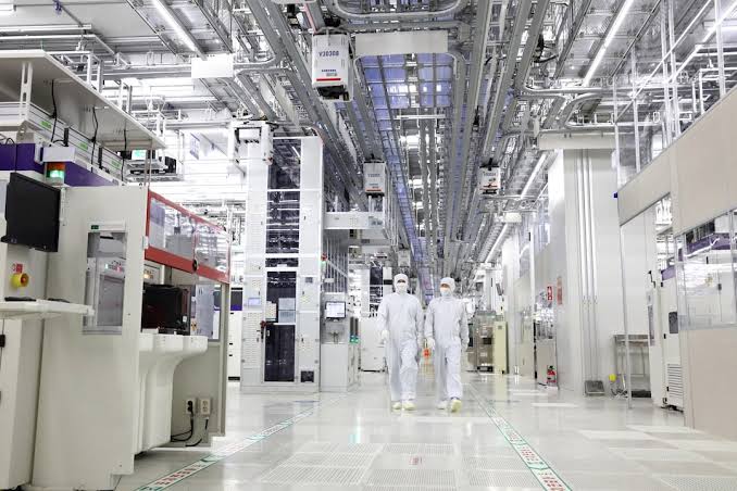
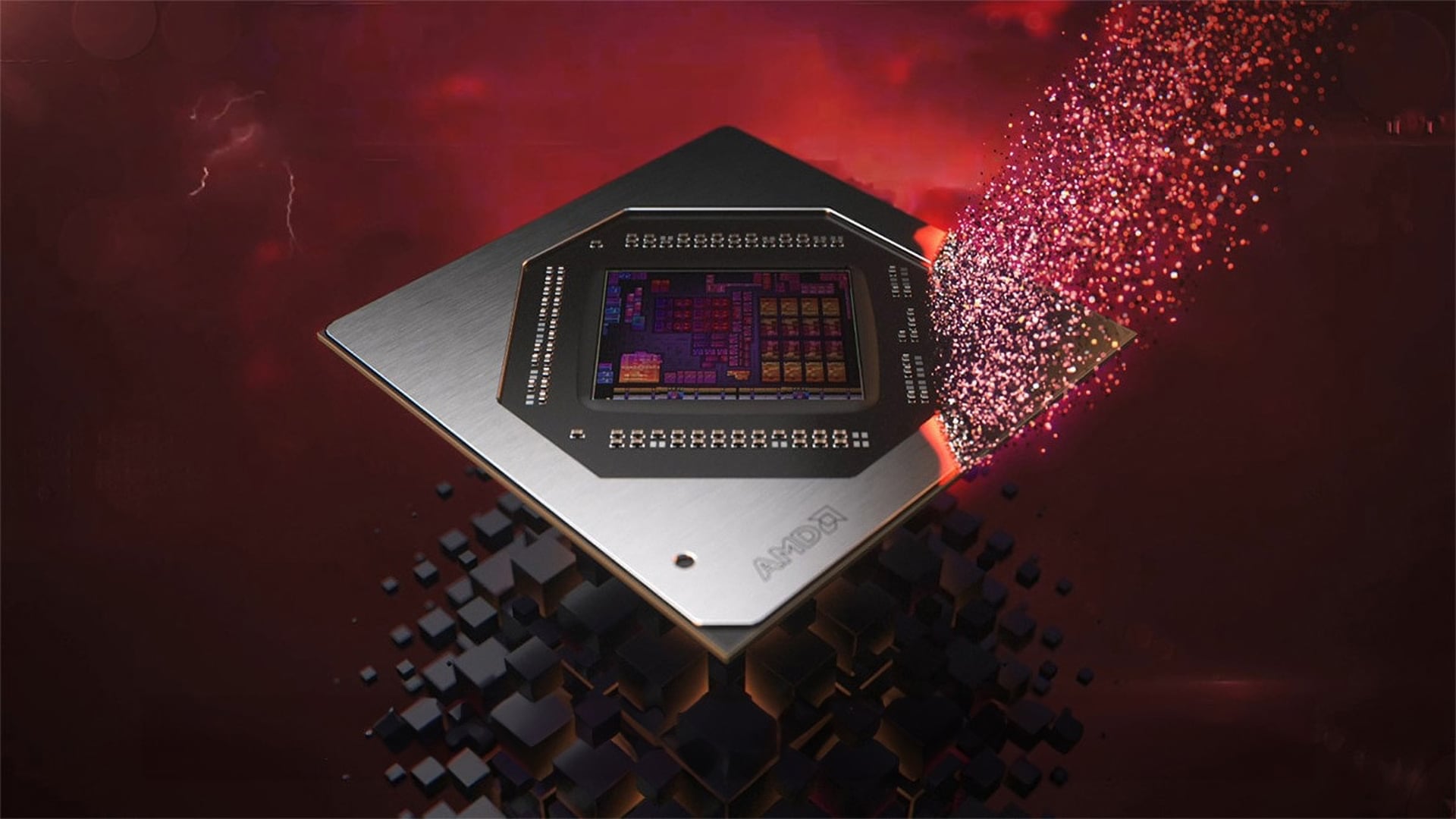
AMD is reportedly preparing to work with Samsung Foundry to manufacture advanced High Bandwidth Memory (HBM) base dies at the company's upcoming Taylor Fab 2 facility in Texas.
The proposed agreement could provide Samsung's semiconductor manufacturing business with a major customer as it expands production capacity in the United States.
According to industry reports, AMD may account for nearly all the production capacity allocated at the new facility. However, neither company has officially confirmed the arrangement.
Samsung is reportedly planning to manufacture the logic base dies in Texas before combining them with DRAM produced at its memory facilities in South Korea.
If confirmed, the agreement would represent an important expansion of Samsung's manufacturing relationship with AMD.
Samsung Taylor Fab 2 Could Begin Mass Production in 2030
Samsung is reportedly progressing with construction preparations for its second semiconductor manufacturing facility in Taylor, Texas.
The new plant is expected to occupy approximately 2.7 million square feet, making it around 1.5 times larger than the company's first Taylor facility.
Reports indicate that ground preparation has been completed and structural construction is beginning.
Samsung is targeting February 2029 for equipment installation, with commercial mass production potentially starting in 2030.
The facility is expected to use Samsung's advanced 2nm manufacturing technology.
| Detail | Reported information |
|---|---|
| Manufacturing facility | Samsung Taylor Fab 2 |
| Location | Taylor, Texas |
| Facility size | 2.7 million square feet |
| Expected technology | 2nm process |
| Equipment installation | February 2029 |
| Commercial production | 2030 |
| Potential major customer | AMD |
The reported production allocation suggests AMD could become a significant customer for Samsung's advanced manufacturing operations.
AMD Partnership Could Strengthen Samsung's HBM Business
HBM is widely used in AI accelerators because it provides high memory bandwidth for demanding computing workloads.
An HBM package includes stacked DRAM chips and a logic base die that helps manage communication with the memory.
Under the reported arrangement, Samsung would manufacture the base dies in Texas and combine them with memory produced in South Korea.
This approach could allow Samsung to provide AMD with more integrated HBM manufacturing services.
However, details concerning production volumes, specific memory generations and contract values remain undisclosed.
Nvidia Reportedly Prefers TSMC for Custom HBM Base Dies
Samsung's potential agreement with AMD comes as Nvidia reportedly favors TSMC for manufacturing custom NVHBM base dies.
Using one semiconductor foundry could help Nvidia maintain consistent memory controller designs and reduce validation requirements across different memory suppliers.
Samsung is nevertheless continuing to develop and validate its own manufacturing processes for advanced HBM components.
The company has also previously secured manufacturing business from Tesla at its first Taylor facility.
If the latest AMD reports prove accurate, Samsung could gain another important customer for its expanding US semiconductor operations.
For now, the proposed partnership remains unconfirmed, with commercial production at Taylor Fab 2 still several years away.

Discussion (0)
Be the first to comment.