

The chip industry is still moving forward, but the pace has changed. A new roadmap linked to IMEC suggests that sub 1nm process technology may not arrive until around 2034, with even smaller 0.2nm class nodes appearing much later, around the 2040s.
That timeline shows how difficult chip scaling has become. For years, new nodes brought regular density improvements. Now, each step needs more complex transistor designs, new materials, advanced packaging, and better power delivery.
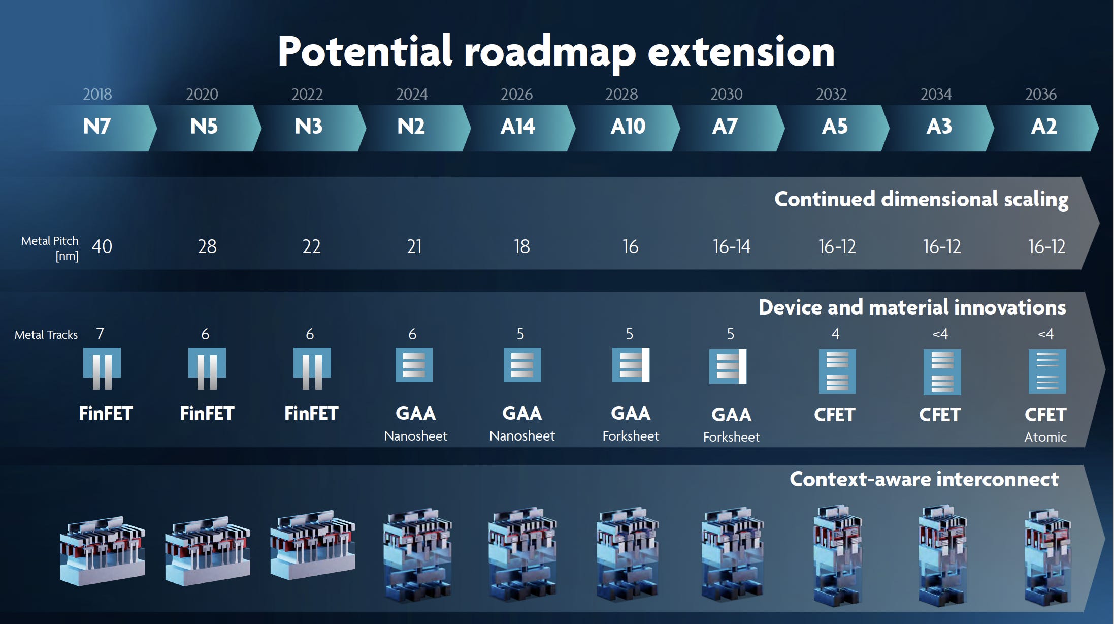
The next big shift starts with nanosheet and CFET designs
The near future belongs to nanosheet transistors, also known as gate all around designs. These are already starting with 2nm class nodes, and they will remain important through several future generations.
After that, the roadmap points to CFETs, or Complementary FETs. These stack transistor structures vertically to save space and improve density. The first CFET based sub 1nm node is expected around 2034, starting with the A7 or 0.7nm class process.
| Expected period | Node class | Main technology |
|---|---|---|
| 2025 | 2nm | Nanosheet GAA |
| 2028 | A14 or 1.4nm | Improved nanosheet |
| 2031 | A10 or 1.0nm | Advanced nanosheet |
| 2034 | A7 or 0.7nm | CFET |
| 2036 | A5 or 0.5nm | Improved CFET |
| 2040 | A3 or 0.3nm | Continued CFET |
| 2043 | A2 or 0.2nm | 2D FET |
| 2046 | Below A2 | Advanced 2D FET |
The roadmap also points to 2D FETs in the 2040s. These would use new channel materials to push miniaturization beyond what silicon based designs can handle easily. The first 0.2nm class process is expected around 2043, followed by sub 0.2nm technology by around 2046.
Packaging and materials now matter as much as transistor size
The slowdown in traditional scaling does not mean chip progress is stopping. It means the industry is finding gains in more places.
Advanced packaging is becoming more important because chiplets let companies combine several pieces of silicon instead of forcing every part onto one huge die. TSMC’s wafer scale packaging and other 2.5D or 3D methods are examples of how companies are increasing compute density without relying only on smaller nodes.
The roadmap also shows major changes in interconnect materials. Copper wiring will become harder to use efficiently at extremely small pitches, so future nodes may move toward materials like ruthenium and, later, alternatives such as platinum cobalt oxide. These changes are meant to reduce resistance and improve conductivity as wiring gets smaller.
Power delivery is also changing. Future chips are expected to move voltage regulation closer to the package, interposer, and even wafer backside. This should help reduce power loss and improve efficiency, especially for AI and high performance computing chips.
The main point is clear. Smaller node names will still matter, but they are no longer the whole story. Future performance will come from several areas working together: transistor design, chiplet packaging, memory placement, interconnect materials, and power delivery.
For you as a normal PC buyer, this roadmap does not mean 0.7nm CPUs are coming soon. These dates refer to research and technology readiness, not immediate retail products. Still, it gives a useful view of where the industry is heading.
The chip roadmap now looks longer and harder than before. Sub 1nm is possible, but it will need new structures and materials to get there. The next two decades of chip progress will be less about simple shrinking and more about smarter ways to stack, connect, and power silicon.


Discussion (0)
Be the first to comment.