

NVIDIA is reportedly moving faster than expected on co packaged optics, with the technology now planned for its Feynman data center GPUs in 2028. Earlier timelines had placed broader commercialization closer to 2033, so this would bring the shift forward by about five years.
Co packaged optics, also called CPO or silicon photonics, replaces more copper based data movement with optical links. The goal is to move data faster, over longer distances, and with lower latency inside large AI systems.
AI factories need faster links than copper can comfortably provide
As AI clusters grow, chips are no longer sitting close together inside one small system. Some deployments can stretch across long distances, while still needing huge amounts of data to move between GPUs, CPUs, networking gear, and storage.
Copper works well at shorter distances, but it becomes harder to scale when bandwidth needs rise and systems spread out. Optical links can help move data at very high speeds with better efficiency across larger AI infrastructure.
| Feynman era feature | Expected role |
|---|---|
| Co packaged optics | Faster data movement using optical links |
| 3D die stacking | Denser GPU packaging and possible stacked compute |
| Custom HBM | Higher memory bandwidth and capacity for AI workloads |
| Rosa CPU | New NVIDIA data center CPU paired with Feynman |
| NVLink 8 CPO | Optical networking for larger AI systems |
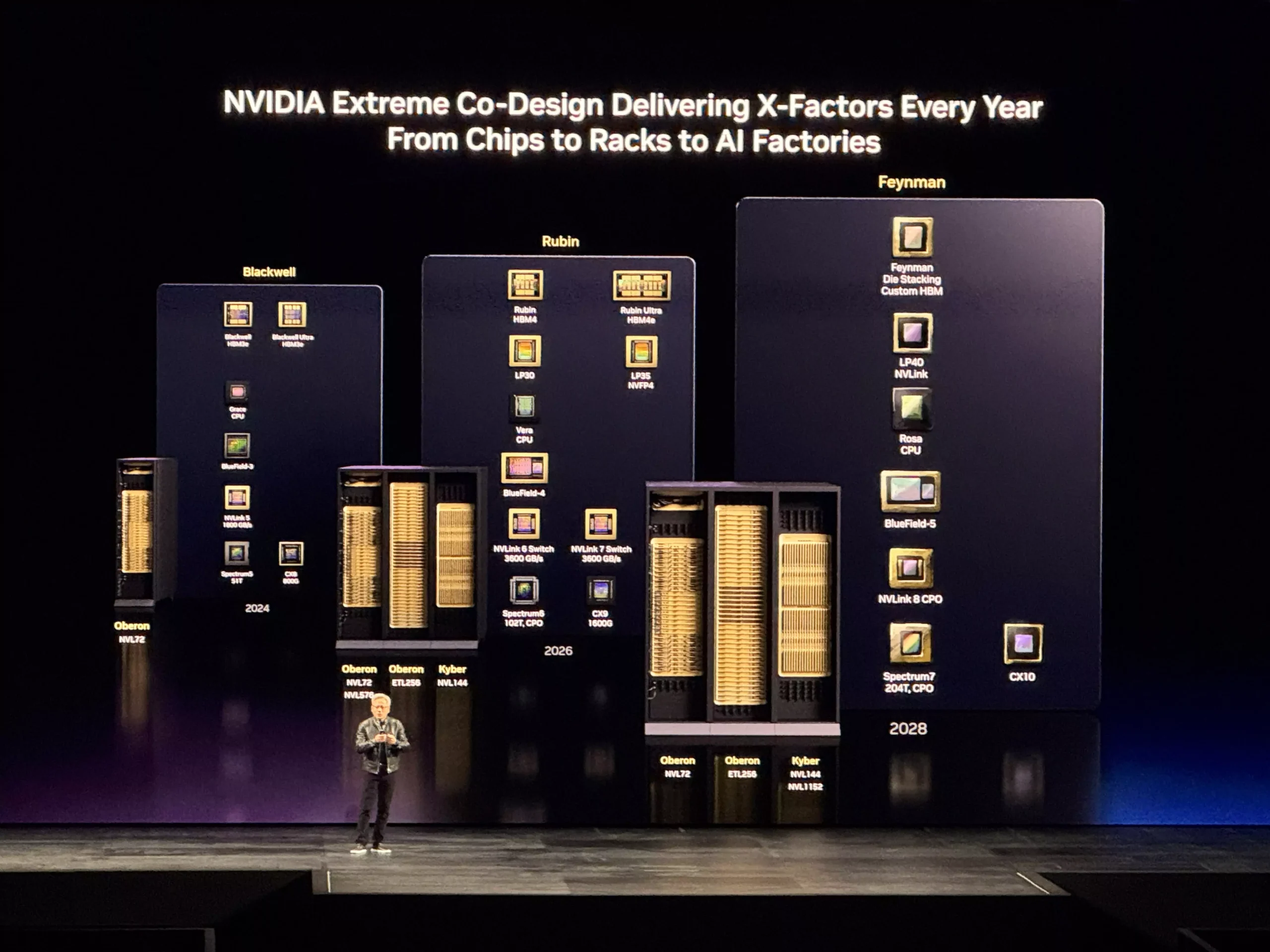
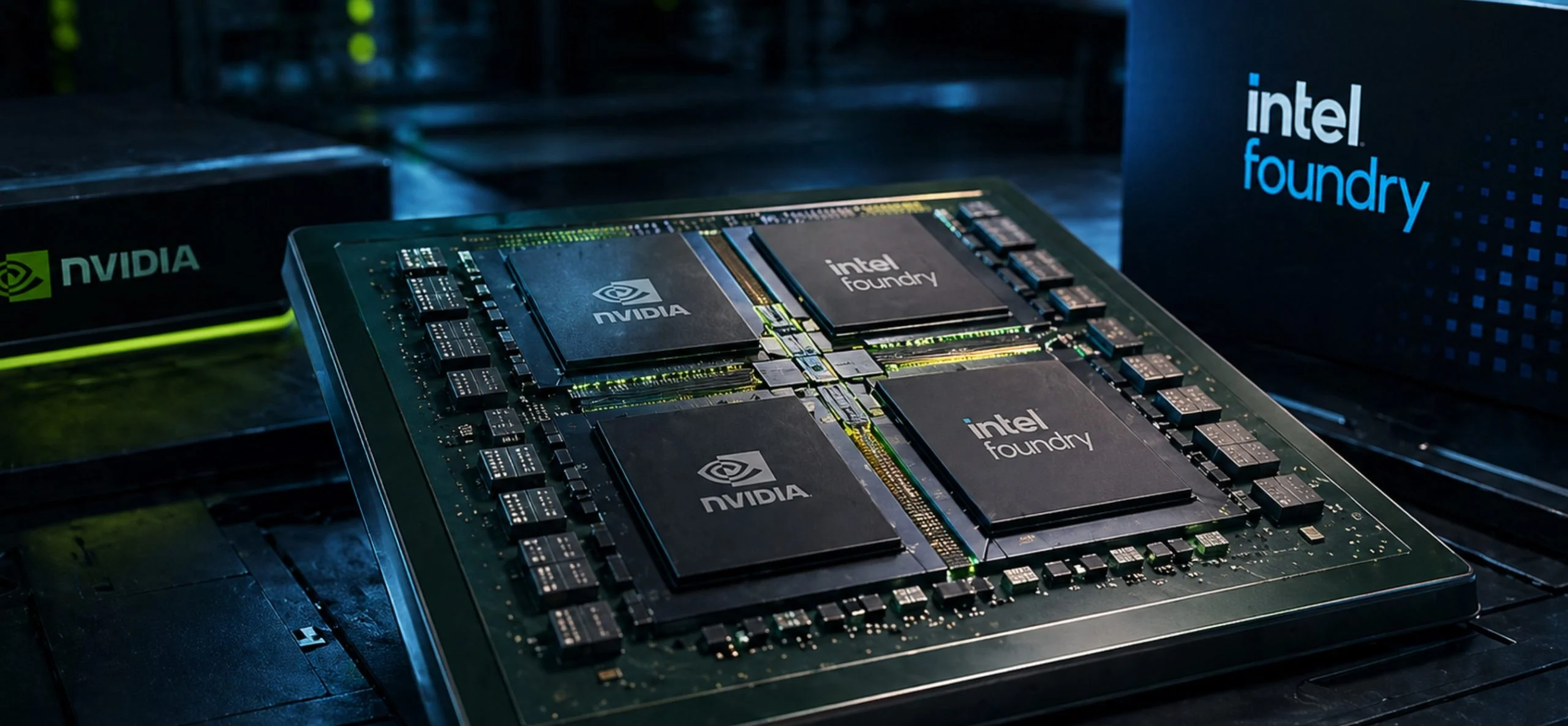
NVIDIA confirmed at GTC 2026 that Feynman will use 3D die stacking. The report also says NVIDIA may use Intel as a foundry partner for advanced packaging, including EMIB, though this remains part of the broader reported roadmap rather than a consumer product announcement.
Memory is another important detail. Feynman is no longer listed with a standard next generation HBM label in the report. Instead, NVIDIA is pointing to custom HBM, which could mean a custom HBM4E variant or something closer to HBM5. That would fit the needs of larger AI systems where memory bandwidth is often as important as raw compute.
Feynman will also move beyond the Vera CPU used with Rubin. NVIDIA’s next data center CPU architecture is called Rosa, named after physicist Rosalyn Sussman. NVIDIA has not shared full details yet, but the change suggests Feynman will be a larger platform shift, not only a GPU refresh.
The move also shows how quickly AI infrastructure is forcing hardware roadmaps to change. CPO was once seen as a longer term technology. NVIDIA now appears to be pulling it into the 2028 generation because large AI clusters need more bandwidth and better system level efficiency.
AMD is reportedly working on its own co packaged optics effort with GlobalFoundries, with a possible first use around its MI500 generation in a similar 2028 window. That suggests optical interconnects may become a major battleground for AI hardware by the end of the decade.
For now, the key point is simple. NVIDIA’s Feynman platform is shaping up to be more than another faster GPU. It may combine optical links, 3D packaging, custom memory, and a new CPU into one system designed for much larger AI factories.


Discussion (0)
Be the first to comment.