



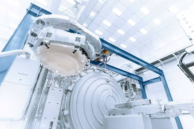
China may be able to produce some advanced semiconductors without access to extreme ultraviolet lithography, but the country will struggle to compete commercially if it continues relying on older deep ultraviolet equipment, according to Zeiss chief executive Frank Rohmund.
Export restrictions prevent companies such as ASML and Zeiss from supplying China with leading EUV systems and related components. Chinese foundries have therefore turned to complex multi patterning techniques using DUV lithography to manufacture chips beyond the normal limits of that equipment.
Rohmund believes this approach can support limited progress, including some 5nm class designs, but only with significant tradeoffs. More patterning steps increase manufacturing complexity, production time, defect risk, and cost. These problems can make advanced chips difficult to produce at high volume and acceptable yields.
His assessment is that China may remain commercially competitive around the 7nm level unless it gains access to EUV technology or develops a domestic alternative that can be used reliably in mass production.
DUV multi patterning can reach smaller nodes but at a high cost
DUV lithography uses longer wavelength light than EUV systems. At advanced process nodes, a single DUV exposure cannot create all the required features, so manufacturers divide the design across several masks and exposures.
This technique is known as multi patterning. It allows foundries to print smaller structures, but every extra step adds cost and increases the chance of alignment errors.
| Manufacturing approach | Main advantage | Main limitation |
|---|---|---|
| EUV lithography | Fewer patterning steps at advanced nodes | Expensive and restricted equipment |
| DUV multi patterning | Uses existing and more widely available tools | Higher cost, complexity, and defect risk |
| Design technology co optimisation | Improves density through design changes | Cannot fully replace advanced lithography |
| Advanced packaging | Combines several dies for higher system performance | Does not solve transistor manufacturing limits |
A foundry may technically demonstrate a 5nm class chip with DUV, but commercial success depends on yield. If too many dies fail during production, the cost of each working chip rises sharply.
Government support can help absorb those costs, especially for strategically important products. However, Rohmund argues that subsidies do not remove the underlying manufacturing disadvantages.
China’s 7nm progress shows both capability and limitations
SMIC has already demonstrated that Chinese manufacturers can push DUV technology further than many expected.
Huawei’s Kirin 9030 is described as using SMIC’s 7nm class N+3 process. The node reportedly uses a tight metal pitch and achieves density characteristics that compare favourably with some processes produced using EUV.
That achievement shows that process labels alone do not provide a complete comparison. A 7nm design from one foundry can have different density, power, performance, and manufacturing characteristics from another company’s 7nm process.
However, density is only one part of the result. Chips must also deliver acceptable performance, energy efficiency, yields, and production volume.
The Kirin 9030 reportedly remains behind leading competitors in performance and power efficiency. This suggests that aggressive design rules and complex patterning can improve density without fully closing the broader technology gap.
EUV becomes more important as nodes shrink
TSMC is moving toward large scale 2nm production, while other major foundries are developing similarly advanced processes.
At these nodes, the number of DUV patterning steps required would become increasingly difficult to manage. More masks and exposures add variation throughout the production process, making consistent yields harder to achieve.
EUV can replace several DUV patterning stages with fewer exposures. This simplifies some parts of production and improves the chance of maintaining commercially viable output.
| Process target | Likely position without EUV |
|---|---|
| 7nm class | Possible at commercial scale with advanced DUV techniques |
| 5nm class | Technically possible but significantly more complex |
| Below 5nm | Increasingly difficult and expensive |
| 2nm class | Unlikely to remain competitive through DUV alone |
| 1.4nm class | Would require major lithography and packaging advances |
China can continue improving chip architecture, design tools, packaging, and materials. These areas may reduce some of the impact of limited lithography access, but they cannot completely replace the ability to manufacture smaller transistors efficiently.
Advanced packaging can extend performance without solving the lithography gap
Huawei has discussed a packaging approach called LogicFolding, which it claims could help create systems with performance associated with much smaller process nodes by 2031.
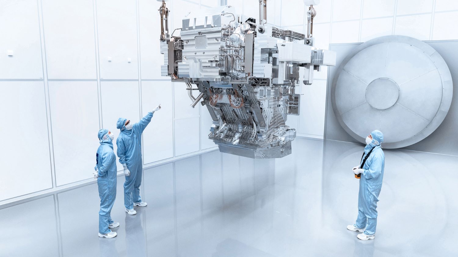
Advanced packaging can combine multiple dies, shorten communication paths, and integrate memory or specialised accelerators more closely. This can improve system performance without requiring every component to use the most advanced manufacturing process.
The approach is already used across the global semiconductor industry. Chiplets and three dimensional stacking allow manufacturers to combine different technologies inside one package.
However, packaging does not eliminate the need for competitive logic production. If the main compute dies consume more power or occupy more space than rival chips, the finished system may still be less efficient.
Manufacturing complexity and yield also remain concerns. Combining several advanced dies increases the number of components that must work correctly inside each package.
Domestic EUV development remains uncertain
Earlier reports claimed that China could begin trial production using domestically developed EUV equipment, but there has been little public evidence confirming meaningful progress toward commercial deployment.
Building an EUV system is an enormous technical challenge. It requires advanced light sources, mirrors, vacuum systems, precision control, metrology, software, and a large supplier network.
Zeiss plays a critical role in producing optical systems for EUV machines, while ASML integrates thousands of components into complete lithography platforms.
China would need to recreate or replace many parts of this ecosystem, not simply build one machine. Even after producing a working prototype, it would need to prove reliability, throughput, accuracy, and compatibility with high volume manufacturing.
Commercial competitiveness depends on more than producing one advanced chip
China may continue demonstrating advanced processors through DUV multi patterning and aggressive design techniques. These achievements are important, but commercial competitiveness requires repeatable production at scale.
A process must produce enough working dies per wafer, operate at predictable costs, and support large customer orders. It must also improve quickly enough to keep pace with rival foundries.
Without EUV, each move to a smaller node is likely to require more complicated manufacturing and heavier financial support.
Rohmund’s view is that DUV can help China maintain progress in the near term, but it is not a sustainable replacement for EUV. Unless domestic lithography efforts succeed, the gap between Chinese foundries and leading global manufacturers may widen as the industry moves deeper into 2nm and later process generations.

Discussion (0)
Be the first to comment.