



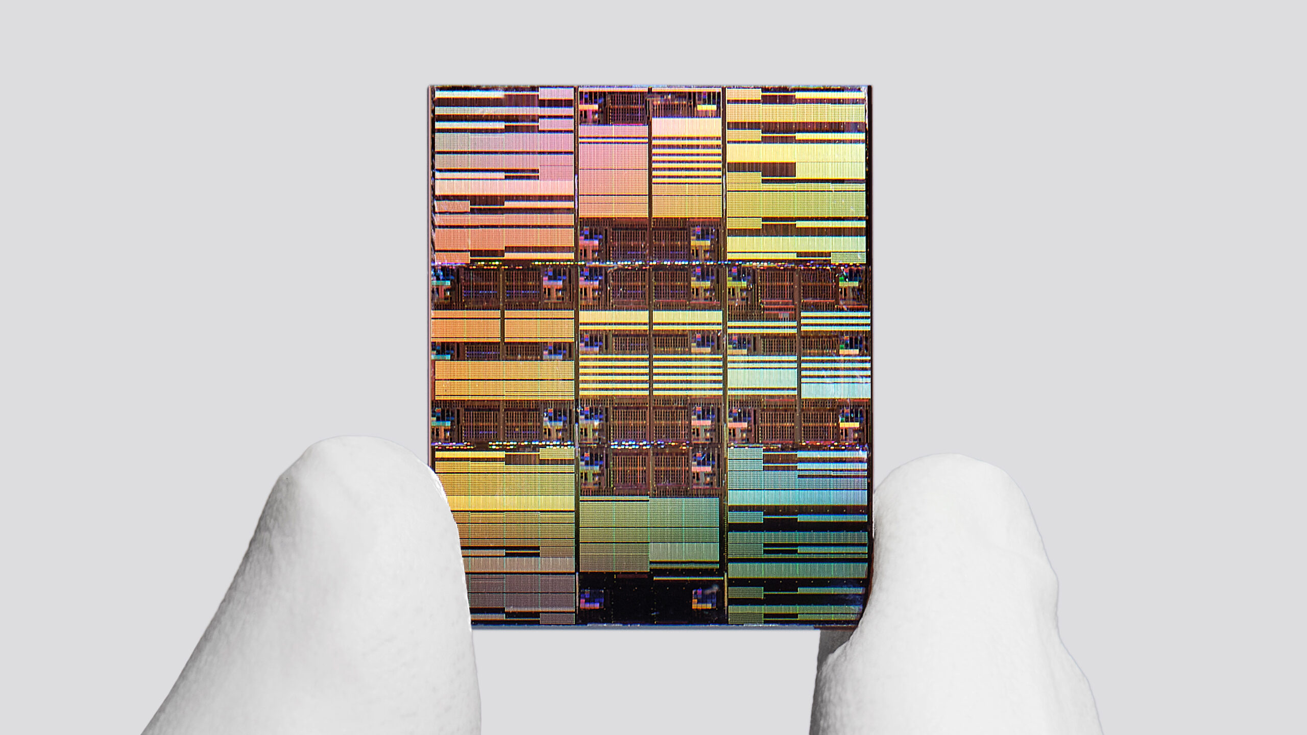
TSMC and university researchers have demonstrated a new transistor design that could help semiconductor manufacturing move toward technologies below 1 nanometer.
The work focuses on one of the biggest problems facing future transistor scaling. As transistor channels become extremely thin and short, controlling the flow of electrons becomes more difficult. Traditional materials and manufacturing techniques start to introduce higher resistance and weaker gate control.
The researchers addressed this problem by changing how the surface of an ultra thin molybdenum disulfide channel is prepared before the transistor's insulating and gate layers are added.
Their approach uses an extremely thin aluminum layer that is deposited directly onto the channel and then oxidized. This creates a smooth aluminum oxide layer that helps the remaining transistor structure form more reliably.
The new transistor approach at a glance
| Area | Detail |
|---|---|
| Channel material | Monolayer molybdenum disulfide |
| Approximate channel thickness | 0.7nm |
| Added aluminum oxide layer | Around 0.42nm |
| Main gate dielectric | High k hafnium oxide |
| Target | Future sub 1nm transistor technologies |
| Main benefit | Better gate control with lower resistance and scattering |
| Research focus | Ultra thin two dimensional transistors |
Today's advanced processors commonly use FinFET or gate all around transistor designs. These structures improve electrical control by allowing the gate to surround more of the transistor channel.
However, there are physical limits to how far conventional silicon based structures can continue shrinking.
When channel lengths approach roughly 3nm to 5nm, controlling electron movement becomes increasingly difficult. Extremely thin channels can also create additional resistance when electrons interact more strongly with surrounding materials.
Two dimensional materials offer one possible solution.
MoS2 offers a naturally thin transistor channel
Molybdenum disulfide, commonly known as MoS2, can form a channel only one molecular layer thick. Its natural thickness is about 0.7nm, making it useful for transistor designs that need to move below the dimensions practical with conventional materials.
A thinner channel gives the gate better control over current flow and could allow chipmakers to continue increasing transistor density.
Manufacturing such thin structures is difficult, however.
Traditional methods for depositing the insulating gate dielectric can create an uneven layer on top of MoS2. That weakens electrical performance and makes it harder to produce reliable transistors at very small dimensions.
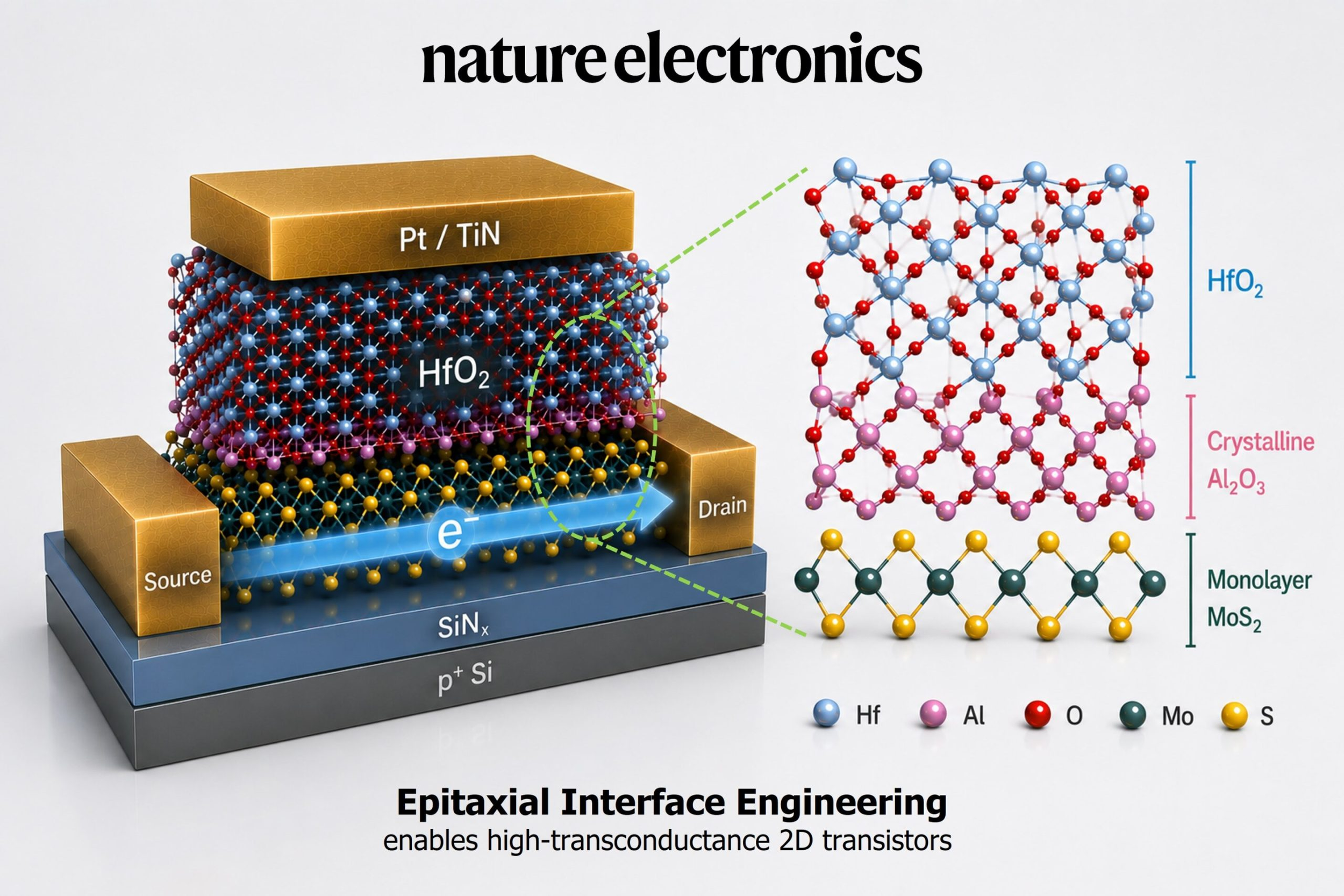
Instead of developing an entirely new dielectric material, the researchers modified the MoS2 surface first.
An ultra thin epitaxial aluminum layer was deposited onto the channel and allowed to oxidize, forming an aluminum oxide film approximately 0.42nm thick. A high k hafnium oxide dielectric was then placed above it.
This intermediate layer creates a more suitable surface for the dielectric and gate structure.
Lower scattering could help future transistor scaling
Testing showed that the engineered interface could provide strong current control while reducing unwanted electron scattering and resistance.
The electrical behavior was comparable with a gate dielectric layer around 1nm thick, despite using an extremely thin interface.
That matters because future transistor development is increasingly limited by interfaces between materials rather than simply by how small chipmakers can print features.
If those interfaces create too much resistance or leakage, reducing transistor dimensions no longer produces useful improvements in power or performance.
The research does not mean commercial sub 1nm processors are ready for production. Moving a laboratory transistor into high volume semiconductor manufacturing requires major work in reliability, repeatability, yield and integration with existing fabrication processes.
Still, the result provides another possible route for extending transistor scaling beyond today's silicon based designs.
TSMC is already preparing advanced manufacturing technologies such as 2nm and 1.4nm for future processors. Research into two dimensional channel materials could eventually become important for generations beyond those nodes.
As conventional transistor dimensions approach their practical limits, controlling materials at the atomic level will become increasingly important. This work shows that carefully engineering the interface around an ultra thin channel could help make that transition possible.


Discussion (0)
Be the first to comment.