



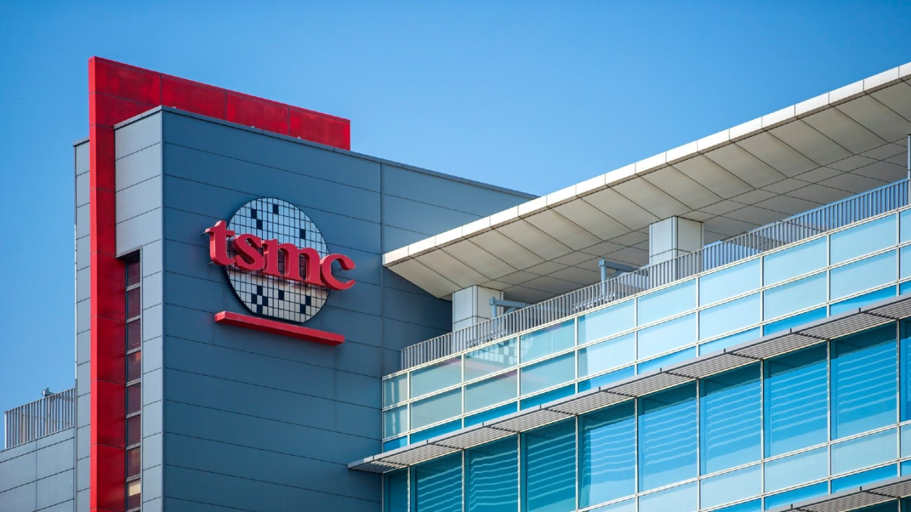
TSMC is reportedly preparing manufacturing capacity for chipmaking technologies beyond its upcoming 1.4 nanometer A14 process, with new facilities planned in Taiwan's Hsinchu Science Park.
A fresh report says the company has secured approval for the third phase of the Longtan Park expansion, where future fabs could eventually produce chips using process technologies smaller than 1.4 nanometers.
The first factory tied to this later phase is expected to begin mass production in 2030.
New fabs would go beyond TSMC's A14 process
TSMC's current leading edge roadmap already includes its 2 nanometer N2 family and the upcoming A14 process.
A14 is expected to deliver meaningful improvements over N2, including higher logic density, better performance and stronger power efficiency.
| Process detail | Reported or expected information |
|---|---|
| Current leading node | N2, 2 nanometer class |
| Next major node | A14, 1.4 nanometer class |
| A14 logic density gain | More than 20 percent versus N2 |
| A14 performance gain | Around 10 to 15 percent |
| A14 power efficiency gain | Around 25 to 30 percent |
| Sub A14 fab target | 2030 mass production |
| Expansion area | About 104 acres |
| Estimated development cost | NT$95 billion, roughly $3 billion |
| Planned factories | Three |
The newly approved expansion is said to include three factories.
According to the report, the first would enter production in 2030, while later facilities would support process technology more advanced than A14.
That suggests TSMC is already planning physical capacity several generations ahead of what is currently in volume production.
Hsinchu expansion was previously delayed
The Longtan expansion has a complicated history.
TSMC had delayed relocation plans in 2023 after local opposition emerged around land acquisition and development.
The project was later revised, with the proposed area reduced from about 159 acres to 104 acres.
Authorities also lowered the amount of privately owned land that would need to be acquired.
The latest approval appears to revive the long term expansion plan with a smaller footprint.
Earlier reports had suggested that the site would initially support two 1.4 nanometer fabs along with a packaging facility.
The newer information now indicates that later stages of the same expansion could move beyond A14.
TSMC and Intel are both pushing toward the next process generations
The timing also highlights the growing competition between TSMC and Intel in advanced semiconductor manufacturing.
Intel is currently working with its 18A process and has outlined 14A as a future generation, with products based on that technology expected around 2028.
TSMC is meanwhile moving from N2 toward A14 and then to technologies below the 1.4 nanometer class.
The naming systems used by the two companies are different, so node labels cannot be compared directly as simple transistor size measurements.
What matters more is the combination of density, power, performance, yield and manufacturing readiness.
Advanced node planning now stretches years ahead
Semiconductor fabs require enormous investments and long construction timelines, so chipmakers need to prepare facilities well before a process reaches mass production.
That is why approval for a 2030 facility can arrive while current products are still focused on 2 nanometer technology.
TSMC's major customers include companies developing processors, GPUs and mobile chips, which means maintaining enough advanced capacity will remain important as demand for AI accelerators and high performance computing continues to grow.
The reported Longtan expansion shows that TSMC is already preparing for the generation after A14 rather than treating 1.4 nanometers as an endpoint.
If the schedule holds, the first fab in the new phase could begin producing sub A14 chips around 2030, extending TSMC's advanced manufacturing roadmap into the next decade.



Discussion (0)
Be the first to comment.