



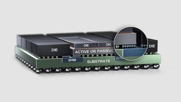
TSMC is reportedly developing a new advanced packaging method inspired by Intel’s EMIB technology as demand for AI chips continues to place heavy pressure on its existing CoWoS production capacity.
The internal project is said to be known as quasi EMIB and is being developed with Kinsus Interconnect Technology. Full technical details have not been disclosed, but the design may use small silicon bridges embedded directly within an organic substrate.
This would reduce reliance on the separate redistribution layer used by TSMC’s current CoWoS L packaging. The simpler structure could lower manufacturing complexity, increase production flexibility and help TSMC serve customers facing long waits for advanced packaging.
The information remains unofficial, and TSMC has not publicly confirmed the project or its expected production schedule.
| Packaging technology | Basic structure | Main characteristic |
|---|---|---|
| CoWoS S | Large silicon interposer | High bandwidth but expensive |
| CoWoS L | Redistribution layer with local silicon bridges | Supports large chip packages |
| Intel EMIB | Silicon bridges embedded in organic substrate | Fewer intermediate layers |
| Reported quasi EMIB | Expected embedded bridge design | Could reduce complexity and cost |
CoWoS demand is exceeding available capacity
Advanced packaging has become an important part of modern AI accelerator production. Large processors often need to communicate with several stacks of high bandwidth memory, requiring fast and dense connections inside a single package.
TSMC’s CoWoS technology is widely used for these products. However, capacity remains heavily constrained, with CoWoS L reportedly sold out through 2026 and extending into 2027.
Lead times have reportedly reached as much as 78 weeks in some cases. These delays can limit how quickly chip designers increase production, even when sufficient wafer manufacturing capacity is available.
Adding another packaging method could help TSMC serve more customers without depending entirely on CoWoS. It could also provide a more economical option for designs that do not require a full silicon interposer or a large redistribution layer.
CoWoS S uses a full silicon interposer
CoWoS S connects processors and high bandwidth memory through a large silicon interposer. This layer sits beneath the main chips and provides a dense network of electrical connections.
The approach supports very high data transfer rates and allows several components to communicate within one package. It has become useful for graphics processors and AI accelerators that need large amounts of memory bandwidth.
Its main disadvantages are cost and manufacturing complexity. Producing a large silicon interposer requires valuable wafer area, and the size of the interposer can limit how large the final package becomes.
The design also uses many micro bumps across the lower surface of the chips. These connections must be manufactured and assembled with high accuracy, adding more steps to production.
CoWoS L reduces dependence on large silicon layers
TSMC developed CoWoS L to address some of the limits of a full silicon interposer.
Instead of placing one large piece of silicon beneath the entire package, CoWoS L uses a redistribution layer as an intermediate carrier. Small local silicon interconnects are positioned only where chiplets need particularly dense connections.
This arrangement combines the high signal density of silicon bridges with the larger and less expensive area available from the redistribution layer.
However, the structure still requires a separate carrier between the chiplets and the organic substrate. The redistribution layer and its embedded bridges must first be manufactured before the complete assembly is attached to the substrate below.
That creates multiple attachment stages and makes the package more complex than Intel’s EMIB design.
Intel EMIB uses bridges directly inside the substrate
Intel’s Embedded Multi Die Interconnect Bridge places small pieces of silicon directly inside an organic package substrate.
The chiplets sit on the substrate and connect across these bridges through dense micro bumps located near their edges. The rest of the package can continue using less expensive organic wiring.
This removes the need for a large silicon interposer or a separate redistribution layer covering the complete package.
| Design area | CoWoS L | Intel EMIB |
|---|---|---|
| Intermediate carrier | Redistribution layer | Not required |
| Silicon connection | Local bridges inside carrier | Bridges inside organic substrate |
| Main attachment process | Multiple assembly stages | More direct attachment |
| Package expansion | Flexible but complex | Localised interconnect design |
| Potential cost | Higher due to extra layer | Lower in suitable designs |
Intel is also developing EMIB T, which adds through silicon vias to the embedded bridges. These vertical channels can carry signals and power from the bottom of the package to processors or memory positioned above them.
This could make the technology useful for more advanced three dimensional chip designs.
TSMC may remove the redistribution layer
The reported quasi EMIB project may place silicon bridges directly inside an organic substrate, following the broad structure of Intel’s approach.
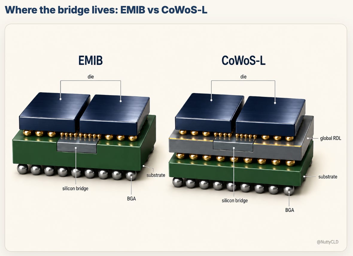
Removing the redistribution layer could simplify manufacturing and reduce the number of attachment stages. It may also lower material costs and allow TSMC to build packages through a production route that is less dependent on existing CoWoS lines.
TSMC could still develop its own implementation rather than copying Intel’s exact structure. Packaging technologies involve different bridge designs, materials, manufacturing methods and intellectual property.
The company’s work with Kinsus may be important because the Taiwanese supplier has experience producing substrates used in advanced semiconductor packages.
Packaging competition is becoming more important
Intel has promoted advanced packaging as one of the strengths of its foundry business. EMIB provides a way to connect chiplets manufactured on different process nodes or by different factories.
TSMC remains the dominant manufacturer of many advanced processors, but limited CoWoS availability creates an opening for competing packaging providers. Customers may look elsewhere if another supplier can offer suitable performance with shorter lead times.
A new embedded bridge solution could help TSMC protect its position while giving customers more choices. It would not necessarily replace CoWoS S or CoWoS L because different chip designs require different packaging methods.
Large AI accelerators may continue using CoWoS, while smaller or more modular products could benefit from an EMIB style approach.
TSMC has not confirmed when quasi EMIB could enter production or which customers might use it. The reported development still suggests that advanced packaging strategy is changing as AI demand pushes current production systems close to their limits.


Discussion (0)
Be the first to comment.