



Tesla is recruiting a Memory Process Integration Engineer for the Terafab semiconductor project, indicating that the planned manufacturing complex could eventually expand beyond logic chips into DRAM and newer memory technologies.
The position covers advanced memory process integration, including DRAM cell development, high volume manufacturing readiness and future technologies such as MRAM, RRAM and 3D DRAM.
That is a significant addition to the scope of Terafab, which is being developed as a highly integrated semiconductor manufacturing operation linked to Tesla and SpaceX.
The project remains at an early stage, so the hiring effort does not mean commercial memory production is close. It does, however, show that memory manufacturing is being considered as part of the longer term roadmap.
Terafab memory role covers full DRAM development
| Area | Planned work |
|---|---|
| Main technology | DRAM |
| Process target | Advanced nodes below 20nm half pitch |
| Cell development | Capacitor and full process integration |
| Manufacturing goal | High volume manufacturing readiness |
| Supporting processes | Etch, deposition, implant and CMP |
| Emerging memory | MRAM, RRAM and 3D DRAM |
| Broader project | Terafab semiconductor complex |
The engineer will be expected to manage the integration of DRAM cell structures from early capacitor design through complete manufacturing flows.
That includes optimizing capacitance density, leakage and refresh behavior, all of which are critical to producing reliable memory at increasingly small dimensions.
The position also involves coordinating with teams responsible for etching, deposition, implantation and chemical mechanical polishing.
Those processes are used to create structures such as wordlines, storage node contacts, capacitor dielectrics and cell plates.
Terafab aims to bring more chip production under one roof
Terafab is designed around a broader strategy of bringing several semiconductor manufacturing steps into one operation.

Plans include areas such as lithography, mask generation, packaging and testing. The stated objective is to reduce the time required to move from chip design to finished hardware.
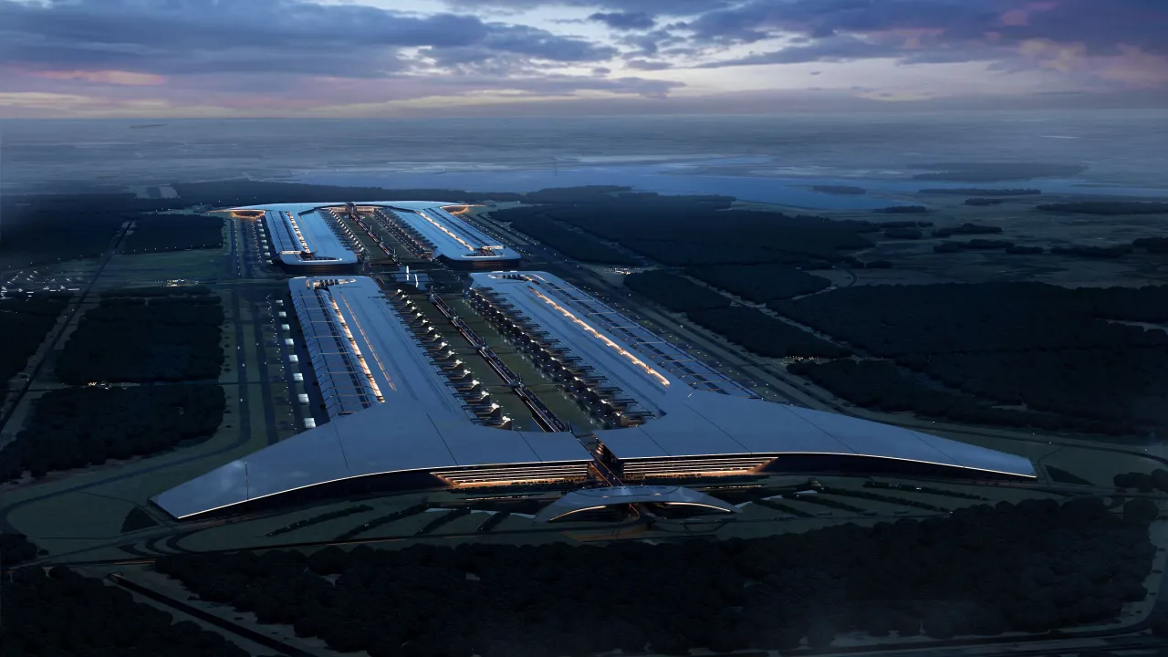
The project is expected to begin with a large semiconductor complex in Grimes County, Texas.
Initial investment has been reported at approximately $16.8 billion, while the proposed site could eventually expand substantially if the broader manufacturing plan is completed.
The longer term ambition is to provide enormous amounts of computing capacity for AI workloads used across Tesla and SpaceX.
Memory would be an important part of that strategy because modern AI systems require large quantities of DRAM and other high bandwidth memory technologies alongside processors and accelerators.
Memory development could reduce dependence on major suppliers
Most advanced DRAM production today is concentrated among a small group of manufacturers, including Samsung, SK hynix and Micron.
Building internal memory manufacturing capability could eventually give Tesla and related companies more control over supply, pricing and technology development.
That does not mean Terafab is ready to compete directly with established DRAM manufacturers.
Developing a commercially competitive DRAM process is extremely difficult. Mature suppliers have decades of manufacturing experience, large patent portfolios and highly optimized production lines.
Yield is another major challenge. A technically functional memory design is only economically useful if enough working dies can be produced from each wafer.
Terafab would therefore need substantial investment, equipment and engineering expertise before it could manufacture memory at meaningful scale.
The roadmap extends beyond conventional DRAM
The job description also mentions MRAM, RRAM and 3D DRAM.
MRAM stores information using magnetic states and can retain data without continuous power. RRAM relies on changes in electrical resistance, while 3D DRAM attempts to increase density by stacking memory structures vertically.
These technologies remain at different stages of commercial maturity, but they could become increasingly important as conventional DRAM scaling becomes more difficult.
Including them in the role suggests Terafab is considering a wider memory research program rather than focusing only on current DRAM architectures.
The immediate importance of the hiring effort is therefore strategic rather than commercial.
Terafab is still being assembled, and there is no confirmed timeline for large scale memory production. However, recruiting engineers specifically for advanced DRAM integration shows that the project is considering memory as a core part of its semiconductor plans.
If that roadmap progresses, Tesla and SpaceX could eventually gain greater control over both compute chips and the memory required to support them, reducing reliance on external suppliers for some of the most important components in future AI infrastructure.

Discussion (0)
Be the first to comment.