



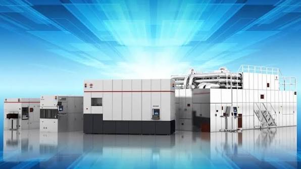
Shanghai Aishengna has reportedly emerged as the company behind China’s latest effort to develop domestic deep ultraviolet lithography equipment.
The company is described as a subsidiary of Shanghai Electric and a sister organisation to Shanghai Micro Electronics Equipment. It is reportedly responsible for immersion DUV systems, while related companies handle other parts of China’s lithography equipment programme.
The reported structure suggests China is dividing the work across several specialised businesses rather than relying on one company to develop every type of machine.
China is also pursuing glass substrates and an early extreme ultraviolet lithography prototype as part of a wider effort to reduce its dependence on restricted foreign semiconductor equipment.
Most details remain unofficial. Production targets, technical performance and commercial readiness have not been independently confirmed.
| Organisation | Reported role |
|---|---|
| Shanghai Aishengna | Immersion DUV lithography |
| Shanghai Micro Electronics Equipment | Krypton fluoride and i line systems |
| AIMES Technology | Supporting and back end lithography equipment |
| Shanghai Electric | Reported parent organisation |
| Huawei and partners | Glass substrate production |
| Separate domestic programme | EUV prototype development |
Aishengna may be preparing domestic immersion DUV machines
Earlier reports claimed that an unidentified Chinese company planned to produce five DUV lithography machines during 2026 and another 20 during 2027.
Initial speculation linked the project to Shanghai Yuliangsheng Technology. New information instead points to Shanghai Aishengna as the company manufacturing the systems.
Aishengna reportedly gained access to patents and technical resources associated with Shanghai Micro Electronics Equipment following a restructuring in 2024.
Under the reported arrangement, Shanghai Micro Electronics Equipment focuses on older lithography technologies, including krypton fluoride systems operating at a wavelength of 248 nanometres and i line equipment covering broader wavelengths.
AIMES Technology reportedly handles equipment used in supporting or later stages of lithography production.
Aishengna is said to focus on immersion DUV equipment, which is more technically demanding and capable of producing smaller features.
Immersion DUV improves optical resolution
DUV lithography uses ultraviolet light to project circuit patterns onto silicon wafers.
Immersion systems place a layer of highly purified water between the final lens and the wafer. Water has a higher refractive index than air, allowing the system to achieve a higher numerical aperture.
This improves resolution and allows manufacturers to print smaller and more closely packed features.
Advanced semiconductor factories can use repeated DUV exposures to produce chips with dimensions smaller than a single exposure would normally permit. However, this method adds cost, complexity and manufacturing time compared with using EUV equipment.
A domestic immersion DUV system could still be valuable for China because it would reduce reliance on imported tools for a broad range of semiconductor products.
It could support mature and selected advanced processes used for memory, processors, power devices and other chips.
Commercial production remains a major challenge
Building an experimental lithography system is different from operating one reliably in high volume manufacturing.
A commercial machine must maintain precise alignment, light output, motion control and optical stability across thousands of wafers. It must also work with photoresists, masks, inspection systems and other equipment inside a complete fabrication process.
Small errors can reduce chip yields and make production uneconomical.
China’s reported target of producing several machines does not confirm that the tools can match systems from established suppliers in accuracy, reliability or throughput.
The programme is therefore unlikely to challenge the leading lithography companies immediately. Its importance lies in creating a domestic technical base that can improve over time.
Glass substrates offer another route to denser chips
China is also reportedly investing in glass substrates as an alternative way to improve processor density and packaging performance.
Huawei is said to be preparing for mass production as early as 2027, while partners establish lines for through glass vias and glass interposers.
Glass substrates can provide better dimensional stability than conventional organic materials. They also resist heat and warping, which becomes increasingly important as chip packages grow larger.
Their smooth surface may support denser wiring, thinner substrates and more precise connections between chiplets.
| Glass substrate benefit | Possible effect |
|---|---|
| Lower warpage | More reliable large packages |
| Better heat resistance | Improved stability under heavy workloads |
| Thin structure | Smaller package height |
| Dense connections | More chiplets and memory links |
| Through glass vias | Vertical signal and power routing |
For large AI processors, these features could help manufacturers combine more compute dies and memory within one package.
Glass substrates do not replace advanced lithography. However, they can improve system performance through packaging even when the individual chips are produced on less advanced process nodes.
This makes the technology useful for a country facing restrictions on leading chip manufacturing tools.
China reportedly has an EUV prototype
China is also reported to have completed an early EUV lithography prototype in Shenzhen.
The project is said to involve former engineers from foreign lithography companies and support from Huawei. Actual chip production using the system is reportedly targeted for 2028.
These claims have not been officially verified, and the technical capability of the prototype remains unknown.
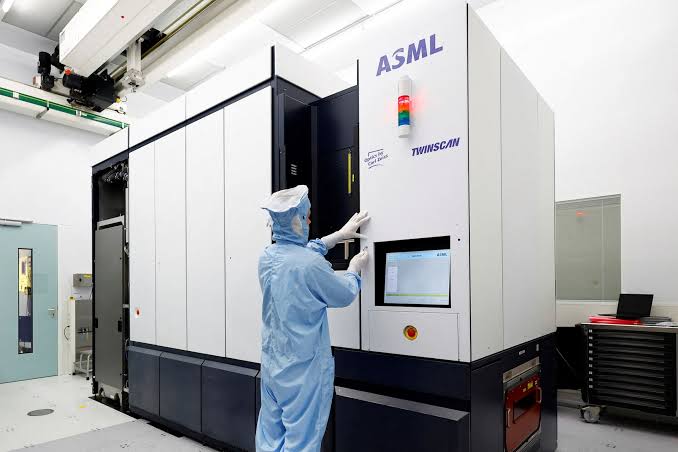
EUV lithography is substantially more difficult than DUV. It requires a powerful 13.5 nanometre light source, extremely precise mirrors, vacuum systems and advanced contamination controls.
Producing a functioning prototype would represent progress, but reaching reliable commercial manufacturing would require further development in many supporting technologies.
The 2028 target should therefore be treated as an ambition rather than a confirmed production schedule.
China is pursuing several paths at the same time
The reported strategy combines three related efforts.
First, domestic DUV equipment could support a wider range of chip manufacturing and reduce dependence on imported tools.
Second, glass substrates could improve chiplet density, thermal performance and package size without requiring every processor die to use the most advanced process.
Third, EUV development represents a longer term attempt to close the gap in leading semiconductor manufacturing.
Each path has different technical risks and timelines. DUV equipment may reach useful production first, while glass substrates could provide benefits through advanced packaging. EUV is likely to remain the most difficult and uncertain programme.
Shanghai Aishengna’s reported role provides a clearer picture of how China may be organising its lithography industry. However, the number of machines produced will matter less than their accuracy, reliability, throughput and ability to support commercially viable chip yields.

Discussion (0)
Be the first to comment.