



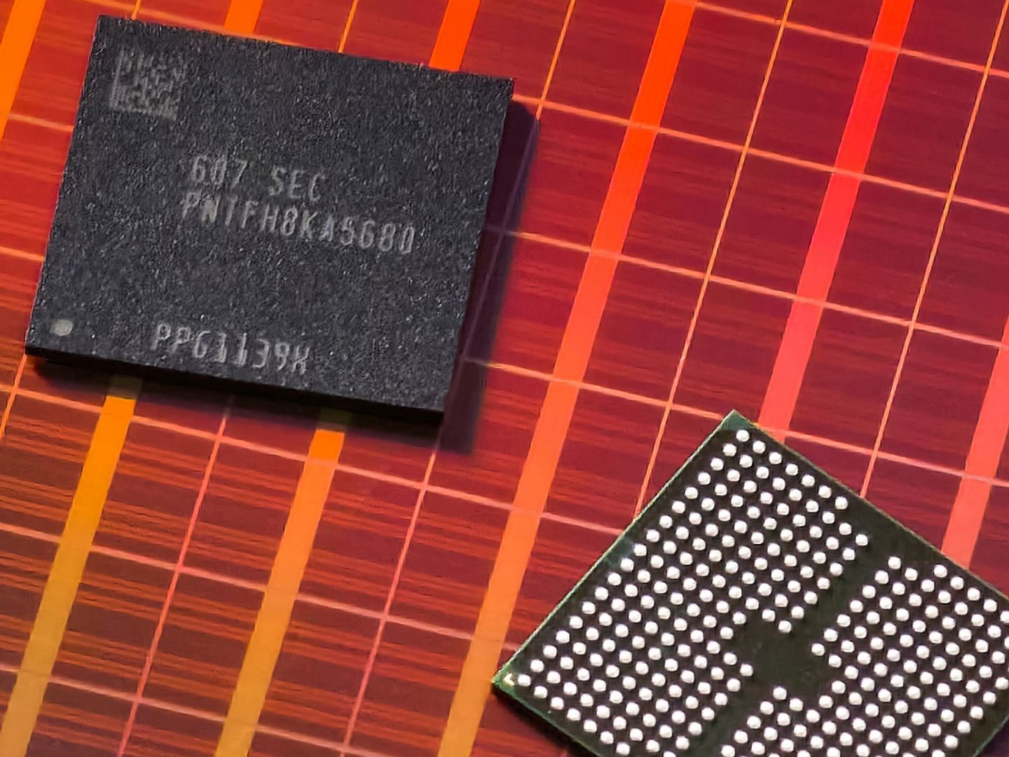
Samsung has introduced several early stage memory and storage technologies designed to address the growing bandwidth, capacity, and power demands of artificial intelligence hardware.
The concepts were shown at FMS 2026 and include zHBM, zNAND-O, and V10 BV-NAND. Samsung is positioning these technologies for future AI accelerators, edge computing devices, and high capacity storage products.
The most ambitious proposal is zHBM, which places high bandwidth memory directly above an AI processor instead of arranging memory stacks beside it. Samsung says this vertical design could reduce package size, shorten data paths, and improve bandwidth and energy efficiency.
V10 BV-NAND focuses on storage. It uses hybrid bonding to build NAND with more than 400 layers while improving density and performance compared with the previous generation.
These technologies remain at different stages of development, and Samsung has not announced commercial release dates or final products.
zHBM Places Memory Directly Above the AI Chip
Current AI accelerators usually place several HBM stacks beside the main processor on a large package.
This arrangement provides high bandwidth, but it consumes significant space and requires data to travel laterally between the processor and memory. Samsung’s zHBM concept instead stacks the memory vertically above the accelerator.
The proposed structure includes the main XPU, an interlayer, the HBM stack, and the package substrate.
| Technology | Main purpose | Proposed benefit |
|---|---|---|
| zHBM | Memory for AI accelerators | Higher bandwidth and smaller package area |
| zNAND-O | High speed edge storage | Lower latency and improved input and output |
| V10 BV-NAND | High density NAND storage | More than 400 layers and better efficiency |
Samsung claims zHBM could deliver eight times the performance of a conventional HBM5 implementation. It also projects more than ten times the memory density, three times the energy efficiency, and a reduction in thermal resistance of more than 50 percent.
These figures are based on Samsung’s concept targets rather than independent testing. The company has not explained the workloads, package sizes, or measurement conditions used for the comparison.
Even so, placing memory closer to the processor could reduce communication delays and improve power efficiency. Data movement is one of the largest sources of energy use in modern AI systems, so shorter connections can provide meaningful benefits.
Vertical Stacking Creates New Cooling Challenges
Placing HBM directly above an AI accelerator may improve bandwidth, but it also makes thermal design more difficult.
Both the processor and memory generate heat. Stacking them vertically can concentrate that heat in a smaller area, making cooling and material selection critical.
Samsung says zHBM could lower thermal resistance, which suggests the design may use specialised bonding layers, heat spreading materials, or cooling structures.
| zHBM challenge | Why it matters |
|---|---|
| Heat concentration | Processor and memory generate heat in the same vertical area |
| Bonding precision | Very small connections must align correctly |
| Manufacturing yield | A defect can affect the full stacked package |
| Repairability | Stacked components are difficult to replace |
| Power delivery | The processor and memory need stable current paths |
| Customer customisation | Different accelerators may require unique layouts |
Samsung says it is already working with customers to refine the technology for future accelerators. The company expects the design to support customer specific implementations rather than one fixed package.
The final success of zHBM will depend on production yield, cooling, cost, and whether chip designers can integrate it into their architectures.
zNAND-O Targets Edge AI Devices
Samsung also introduced zNAND-O, a high performance storage concept based on its existing V-NAND technology.
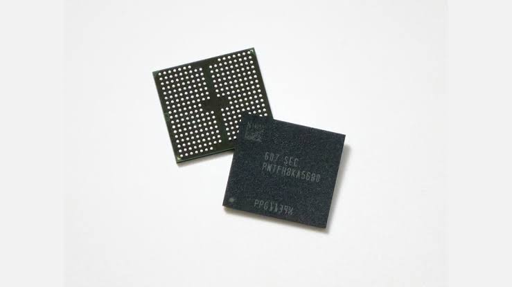
The design is planned in four layer and eight layer configurations. It is intended to provide higher input and output performance, lower latency, and better use of physical space.
Samsung is positioning zNAND-O for edge AI applications. These systems process data closer to where it is generated instead of sending every task to a remote data centre.
Examples could include robotics, industrial systems, vehicles, cameras, and local AI servers.
| zNAND-O feature | Expected role |
|---|---|
| Four and eight layer designs | Provides different capacity and performance options |
| Low latency | Speeds access to stored data |
| Higher I/O performance | Supports demanding AI workloads |
| Compact design | Saves space in edge devices |
| V-NAND foundation | Builds on established Samsung storage technology |
The company has not confirmed whether zNAND-O is connected to its longer term plans for multi-stack NAND expected around 2030.
No capacity figures, controller specifications, endurance ratings, or launch schedule were provided.
V10 BV-NAND Moves Beyond 400 Layers
V10 BV-NAND is Samsung’s next generation NAND architecture and its first to use hybrid bonding.
Traditional NAND development has focused on increasing the number of layers within one structure. As those stacks become taller, manufacturing becomes more difficult because the channels running through the memory must remain precise across hundreds of layers.
Hybrid bonding allows Samsung to combine separately manufactured structures with dense electrical connections.
This approach can increase capacity without relying only on one extremely tall monolithic stack.
| V10 BV-NAND detail | Samsung claim |
|---|---|
| Layer count | More than 400 layers |
| Bonding method | Hybrid bonding |
| Density improvement | 58 percent over V9 NAND |
| Performance | Higher read and write speeds |
| Efficiency | Improved power use |
| Long term direction | Path toward 1,000 layer NAND |
Samsung says V10 BV-NAND offers a 58 percent increase in memory density compared with V9 NAND. It also claims improvements in reading, writing, and general input and output performance.
The company has not provided exact speed or energy consumption figures.
Hybrid Bonding Could Enable 1,000 Layer NAND
Samsung is already discussing NAND designs with more than 1,000 layers.
Reaching that level through conventional stacking alone would create major manufacturing challenges. Taller structures require deeper channel holes, stricter alignment, and more complex materials.
Hybrid bonding allows several NAND sections to be produced separately and then joined. This can reduce some of the difficulties associated with manufacturing one extremely tall structure.
The technique may also allow Samsung to combine memory arrays and control circuits more efficiently.
| Traditional approach | Hybrid bonded approach |
|---|---|
| Builds one increasingly tall stack | Joins separately manufactured structures |
| Requires very deep channel holes | Reduces dependence on one deep structure |
| Higher difficulty as layers increase | May scale more effectively |
| Limited flexibility | Allows more modular designs |
| Yield can decline with height | Defects may be isolated before bonding |
Hybrid bonding is not automatically cheaper. It adds precision bonding steps, inspection requirements, and new production equipment.
Samsung will need to show that the density and performance improvements justify the added manufacturing complexity.
AI Demand Is Driving Faster Memory Development
AI accelerators require large amounts of memory that can move data quickly while using as little power as possible.
The processor alone cannot deliver strong performance if it spends too much time waiting for model weights or other data. This makes memory bandwidth, capacity, and placement increasingly important.
Samsung is developing several products for this market, including HBM4E, HBM5, GDDR7, zHBM, and advanced NAND.
| AI requirement | Relevant Samsung technology |
|---|---|
| Very high memory bandwidth | HBM4E, HBM5, and zHBM |
| High capacity storage | V10 BV-NAND |
| Low latency local storage | zNAND-O |
| Graphics and accelerator memory | GDDR7 |
| Better package density | Vertical zHBM stacking |
| Future storage scaling | Hybrid bonded NAND |
The company is trying to improve both working memory and long term storage. AI systems need HBM for active processing and NAND for model storage, datasets, checkpoints, and local caching.
Samsung’s concepts address both areas, although their commercial readiness remains uncertain.
Commercial Deployment Will Take Time
The technologies shown at FMS 2026 are not all ready for immediate production.
zHBM appears to be a concept under development with selected customers. zNAND-O also lacks a confirmed product schedule. V10 BV-NAND is more clearly connected to Samsung’s storage roadmap, but the company has not announced when consumer or enterprise SSDs will use it.
The biggest questions involve manufacturing yield, cooling, cost, reliability, and compatibility with customer processors.
Samsung’s proposals show how memory architecture may change as AI chips become larger and more demanding. Instead of placing every component beside the processor, future packages may rely increasingly on vertical integration.
If Samsung can deliver its stated improvements, zHBM could significantly increase memory density and bandwidth for AI accelerators, while V10 BV-NAND could provide higher capacity storage without relying on a single extremely tall NAND stack.


Discussion (0)
Be the first to comment.