



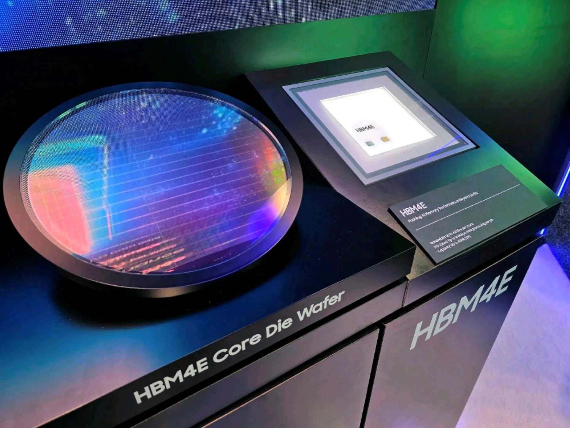
Samsung is reportedly preparing to begin large scale production of high bandwidth memory using hybrid bonding in 2029 or 2030, a schedule that could align the technology with NVIDIA’s future Feynman AI accelerators.
Hybrid bonding is considered an important next step for HBM manufacturing because it removes the small metal bumps traditionally used to connect stacked DRAM layers. This allows the layers to sit closer together, which can improve signal quality, reduce power consumption, and support denser memory designs.
Samsung is expected to install its first hybrid bonding equipment at its Pyeongtaek production facilities by the end of 2026. However, full commercial output may not begin for another three to four years as the company prepares manufacturing processes and improves production yields.
The timing suggests that Samsung may introduce hybrid bonding with HBM4E or a later generation such as HBM5, rather than using it extensively with current HBM products.
Hybrid bonding could improve future HBM performance
Current HBM stacks rely on through silicon vias and micro bumps to connect several DRAM layers vertically. This structure provides much higher bandwidth than conventional memory, but the physical connections take up space and can create limits as manufacturers add more layers.
Hybrid bonding replaces the micro bump connections with direct copper connections between the bonded surfaces. The reduced spacing can make the complete memory stack thinner and allow more electrical connections within the same area.
| Technology detail | Reported information |
|---|---|
| Manufacturing method | Hybrid bonding without conventional micro bumps |
| Initial equipment installation | Expected by the end of 2026 |
| Full scale production | Expected in 2029 or 2030 |
| Main Samsung facility | Pyeongtaek |
| Equipment order | Around 50 hybrid bonding machines |
| Possible memory generation | HBM4E, HBM5, or a custom design |
| Potential GPU generation | NVIDIA Feynman |
The technology may also improve thermal performance because the shorter connections can reduce electrical resistance. This will become increasingly important as AI accelerators use larger and faster HBM stacks.
However, hybrid bonding is more difficult to manufacture than conventional stacking. The surfaces must be extremely clean and accurately aligned, and a defect in one layer can affect the entire stack.
Samsung is reportedly buying around 50 bonding machines
Samsung is said to be acquiring approximately 50 hybrid bonding systems from Dutch semiconductor equipment company BE Semiconductor.
The company reportedly wants modifications to the standard equipment, which may encourage it to purchase additional machines from South Korean suppliers. Locally developed tools could give Samsung more control over the manufacturing process and reduce dependence on a single overseas vendor.
Installing equipment is only the first step. Samsung must test the machines, qualify materials, establish reliable production processes, and improve yields before commercial shipments can begin.
HBM stacks contain many advanced components, so low yields can make each completed product extremely expensive. Samsung is therefore likely to increase production gradually rather than moving directly to high volume output.
Feynman may use custom next generation HBM
NVIDIA’s Feynman architecture is expected to follow Rubin Ultra in the company’s AI accelerator roadmap.
NVIDIA has indicated that Feynman will use advanced three dimensional packaging and custom high bandwidth memory. Intel is also expected to participate as a packaging partner.
Rubin Ultra is currently associated with HBM4E, so Feynman could move to HBM5 or a specially designed memory product that differs from standard HBM specifications.
The reported 2029 production target for Samsung’s hybrid bonding HBM broadly matches the expected period for Feynman systems. This does not confirm that Samsung has secured NVIDIA orders, but it shows that the manufacturing plans could support that generation of accelerators.
Custom memory is becoming more important as AI chipmakers optimise complete systems rather than purchasing standard components. A custom HBM design can be adjusted for capacity, bandwidth, power efficiency, and communication with a specific accelerator.
Custom HBM replaces the standard base die
One important part of Samsung’s reported plans involves custom HBM.
A conventional HBM stack contains several DRAM layers placed above a base die. In a custom design, the standard base die can be replaced with a logic die created for a particular customer.
This logic component can handle memory management, communication, data movement, or other functions that would normally take place elsewhere in the system.
| HBM design | Base layer |
|---|---|
| Standard HBM | Conventional memory base die |
| Custom HBM | Customer specific logic die |
| Main benefit | Closer integration with the accelerator |
| Possible uses | Data movement, memory control, specialised processing |
Combining a custom logic die with hybrid bonding could create a more tightly integrated three dimensional package. This may reduce latency and improve efficiency between the memory and AI processor.
The approach could also allow chip companies to differentiate their systems even when using memory supplied by the same manufacturer.
The delay reflects the difficulty of the transition
A 2029 or 2030 target does not necessarily mean Samsung is falling behind. Hybrid bonding requires major changes to equipment, materials, testing, and production methods.
The company must ensure that the technology works reliably across stacks containing many layers. It must also keep costs competitive with mature micro bump manufacturing.
Samsung faces competition from SK hynix and Micron, both of which are expanding HBM capacity as demand from AI companies continues to rise. The supplier that can introduce reliable hybrid bonding at high volume may gain an advantage in later memory generations.
At the same time, customers will not adopt the technology simply because it is newer. Hybrid bonded HBM must provide enough improvement in bandwidth, capacity, efficiency, or packaging density to justify the added manufacturing complexity.
Samsung’s reported schedule places commercial production near the end of the decade, when AI accelerators are expected to require even larger memory pools and faster data movement. If the company can improve yields and complete its equipment rollout on time, hybrid bonding may become a central part of its HBM strategy for Feynman era systems and the generations that follow.


Discussion (0)
Be the first to comment.