




Samsung is reportedly considering using its 2nm process technology to manufacture base logic dies for future HBM memory, potentially extending its roadmap beyond the 4nm base dies planned for HBM4.
The company may repurpose part of an under construction research and development facility in South Korea for this work. The plans are still preliminary and could change because the facility is not expected to open for roughly two years.
According to the report, the potential 2nm base dies could be aimed at HBM products supplied for NVIDIA AI accelerators.
HBM base dies are becoming more advanced
| Area | Detail |
|---|---|
| Current Samsung HBM4 base die plan | 4nm |
| Reported future option | 2nm |
| Possible production location | Giheung, South Korea |
| Reported line | NRD K Line 2 |
| Potential customer | NVIDIA |
| Status | Reported, not officially confirmed |
| Expected facility timing | Roughly two years |
HBM packages stack several DRAM dies vertically to provide high memory bandwidth in a compact footprint.
The base die sits underneath those memory layers and handles important logic and communication functions. As HBM data rates increase and interfaces become wider, the requirements placed on this logic die also become more demanding.
Earlier HBM generations used relatively mature logic processes. With HBM3 and HBM3E, base dies began moving toward foundry processes in the range of roughly 20nm to 12nm as pin speeds and bandwidth increased.
HBM4 represents another major step because it uses wider interfaces and a larger number of Through Silicon Vias.
Samsung could move beyond its planned 4nm HBM4 design
Samsung previously said it would use a 4nm manufacturing process for HBM4 base dies.
The new report suggests the company is now examining a further move to 2nm for later HBM products.
That would place the base logic on a much more advanced process, potentially allowing Samsung to improve transistor density, power efficiency and logic capability.
However, the report does not confirm which HBM generation would use the 2nm base die or when commercial production might begin.
The plan is therefore better viewed as a possible extension of Samsung's HBM roadmap rather than a confirmed product announcement.
NVIDIA could be a target customer
The reported 2nm base die effort may be intended for HBM products supplied to NVIDIA.
NVIDIA's newer AI accelerators require increasingly large amounts of memory bandwidth and capacity, which has pushed HBM development forward rapidly.
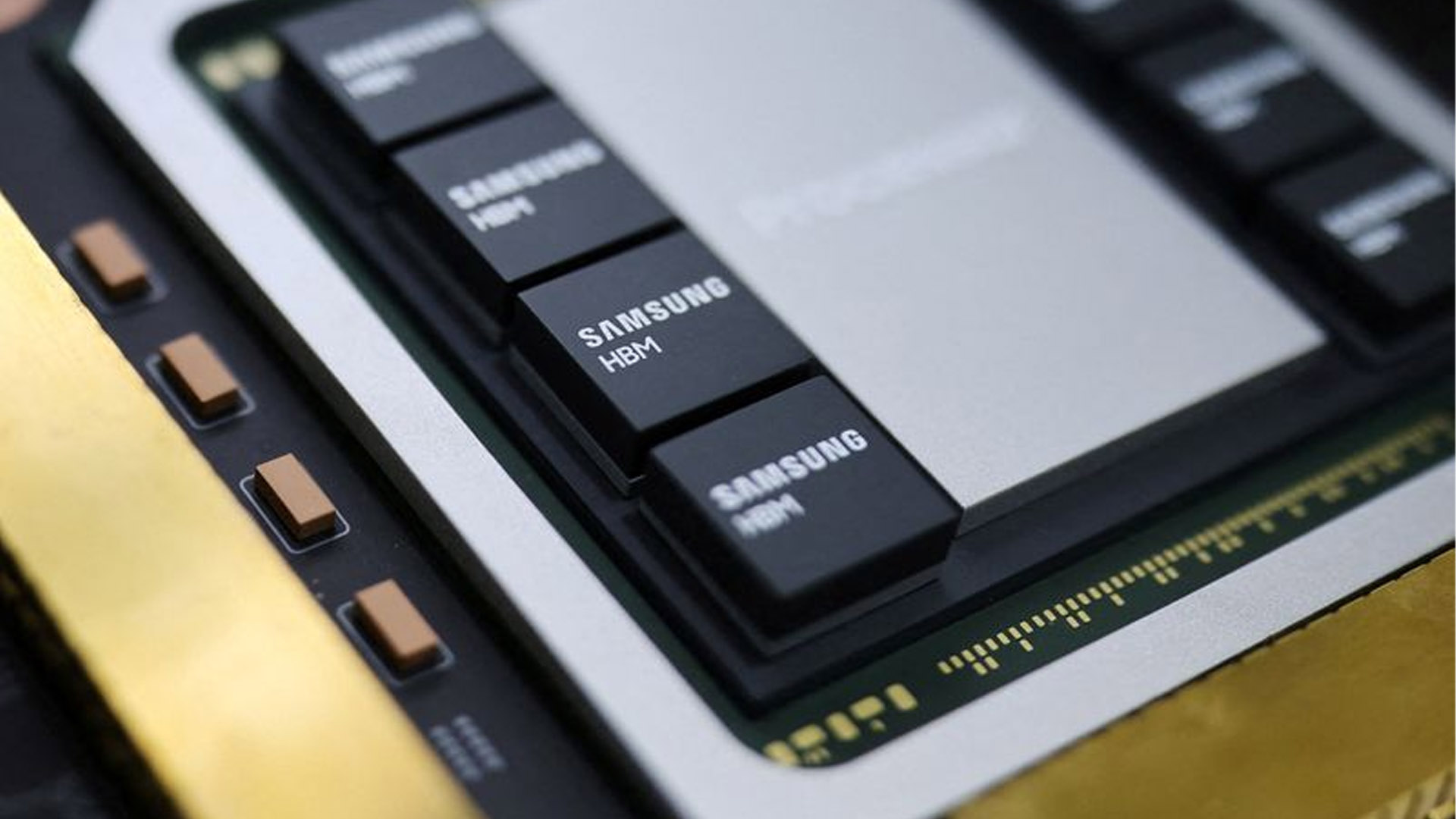
HBM4 is already being adopted for the latest generation of AI hardware, including NVIDIA's Rubin platform.
Moving the base die to a more advanced logic node could give memory manufacturers additional room to add functions and support higher performance as future accelerator designs become more complex.
Foundries are taking a larger role in HBM production
The change also reflects a broader shift in the HBM industry.
As base dies become more complex, memory companies are increasingly relying on advanced foundry processes rather than handling every part of HBM production internally.
Samsung has its own foundry business, giving it the option to manufacture advanced base dies within the company.
SK hynix, meanwhile, has partnered with TSMC for HBM base die production. TSMC offers both mature and advanced process options for HBM related logic.
Micron has also partnered with TSMC for its HBM4 products.
This makes the base die another important area of competition between HBM suppliers, alongside DRAM stacking, packaging, bandwidth and capacity.
Samsung's reported 2nm plan remains subject to change, but it shows how quickly HBM architecture is evolving. If the company moves ahead, future HBM products could combine advanced stacked DRAM with base logic manufactured on one of Samsung's most advanced process nodes.


Discussion (0)
Be the first to comment.