




Samsung has reportedly developed its first 900 layer V NAND prototype, bringing the company closer to its long term goal of 1000 layer NAND. The new prototype uses Cell Multi Bonding technology, which combines two 450 layer cell stacks into one integrated device.
This is not repeated news. It connects to the wider memory shortage and NAND supply discussion, but the main update is new: Samsung has reached a 900 layer V NAND prototype and is moving closer to 1000 layer storage technology.
Samsung’s stacked approach could help future SSDs reach much higher capacities
V NAND is the type of memory used in SSDs and many other storage products. More layers usually mean more storage capacity can be packed into the same physical space. That matters for data centers, AI systems, laptops, desktops, phones, enterprise servers, and consumer SSDs.
| Detail | Information |
|---|---|
| Company | Samsung |
| Technology | 900 layer V NAND prototype |
| Method | Cell Multi Bonding |
| Structure | Two 450 layer cell stacks combined |
| Main benefit | Higher storage density |
| Future target | 1000 layer V NAND |
| Expected 1000 layer timing | Around 2030 |
Samsung reportedly used Cell Multi Bonding, or CMB, to create the 900 layer prototype. Instead of building one extremely tall stack at once, the company bonded two 450 layer wafers together. This approach could help Samsung move toward much denser NAND without relying only on increasing a single stack’s height.
That does not mean mass production is close. The technology is still in prototype form, and Samsung still has major engineering problems to solve before products based on this approach reach the market. One of the biggest challenges was wafer warping, which can happen when very tall NAND structures become difficult to keep stable. Samsung reportedly addressed this with an Upper Chuck Design. The company also worked on misalignment problems using Overlay Correction technologies.
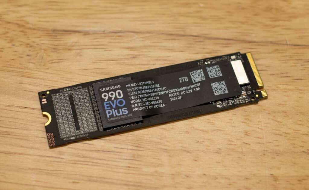
The timing is important because NAND makers are under pressure from both traditional storage demand and AI related growth. AI systems need enormous amounts of fast storage, and data centers are pushing for higher capacity SSDs. If Samsung can make 900 layer and eventually 1000 layer NAND practical, future drives could offer much more capacity without needing larger physical designs.
Samsung is not alone in this race. SK Hynix currently leads with 321 layer NAND and is already working toward 400 layer technology. Samsung is also moving toward 400 plus layer NAND in the coming years, while SK Hynix is using hybrid bonding methods and Samsung is using vertical bonding approaches. Chinese company YMTC is also moving quickly, with 294 layer and 232 layer NAND products already in its lineup.
The competition matters because the NAND market is becoming more strategic. Storage is no longer only about consumer SSD prices. It is now tied to AI data centers, cloud infrastructure, smartphones, PCs, and enterprise systems. Higher density NAND could help ease capacity pressure over time, but only if manufacturers can scale production reliably.
Samsung’s 900 layer prototype is best seen as a technology milestone rather than an immediate product announcement. It shows that the company has a path toward 1000 layer NAND, but commercial products will still take time. The report says 1000 layer V NAND is currently aimed for around 2030, while 400 plus layer products are expected earlier.
For now, the news shows how quickly storage technology is evolving. Samsung has taken a major step beyond today’s production NAND, and the industry is moving toward SSDs with far higher density in the next few years.


Discussion (0)
Be the first to comment.