



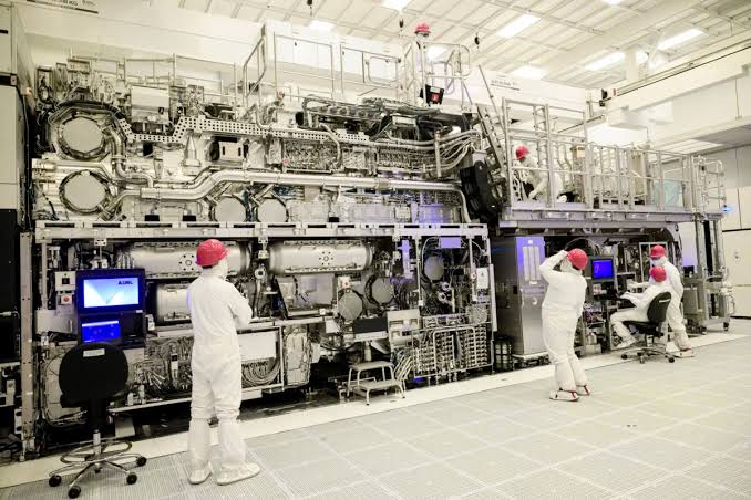
Samsung plans to introduce High NA EUV lithography for its 1nm class process technology rather than using the expensive machines for earlier 2nm or 1.4nm nodes.
The change reflects a more cautious approach to ASML’s newest lithography systems, which use a higher numerical aperture to print smaller chip features. Samsung had previously expected to use High NA EUV for volume production at more advanced nodes before 1nm, but the company now believes the technology will become necessary starting around its A10, or 1nm, generation.
Mass production using the machines could begin around 2030.
Samsung shifts High NA EUV to later nodes
| Detail | Current plan |
|---|---|
| High NA EUV introduction | Around 1nm class production |
| Earlier expected use | 2nm and 1.4nm |
| Numerical aperture | 0.55 NA |
| Possible mass production timing | Around 2030 |
| Main benefit | Smaller patterns with fewer patterning steps |
| Main reason for delay | Technology maturity and cost considerations |
Samsung’s decision follows a similar pattern to TSMC, which has also explored ways to extend conventional EUV further before adopting High NA systems more broadly.
High NA EUV can reduce multi patterning
Current EUV lithography systems use 13.5nm wavelength light. As chip features shrink, manufacturers need increasingly complex techniques to print smaller structures accurately.
High NA EUV improves resolution by increasing the numerical aperture of the optical system.
ASML’s High NA machines use a 0.55 numerical aperture, compared with lower NA systems used in current production.
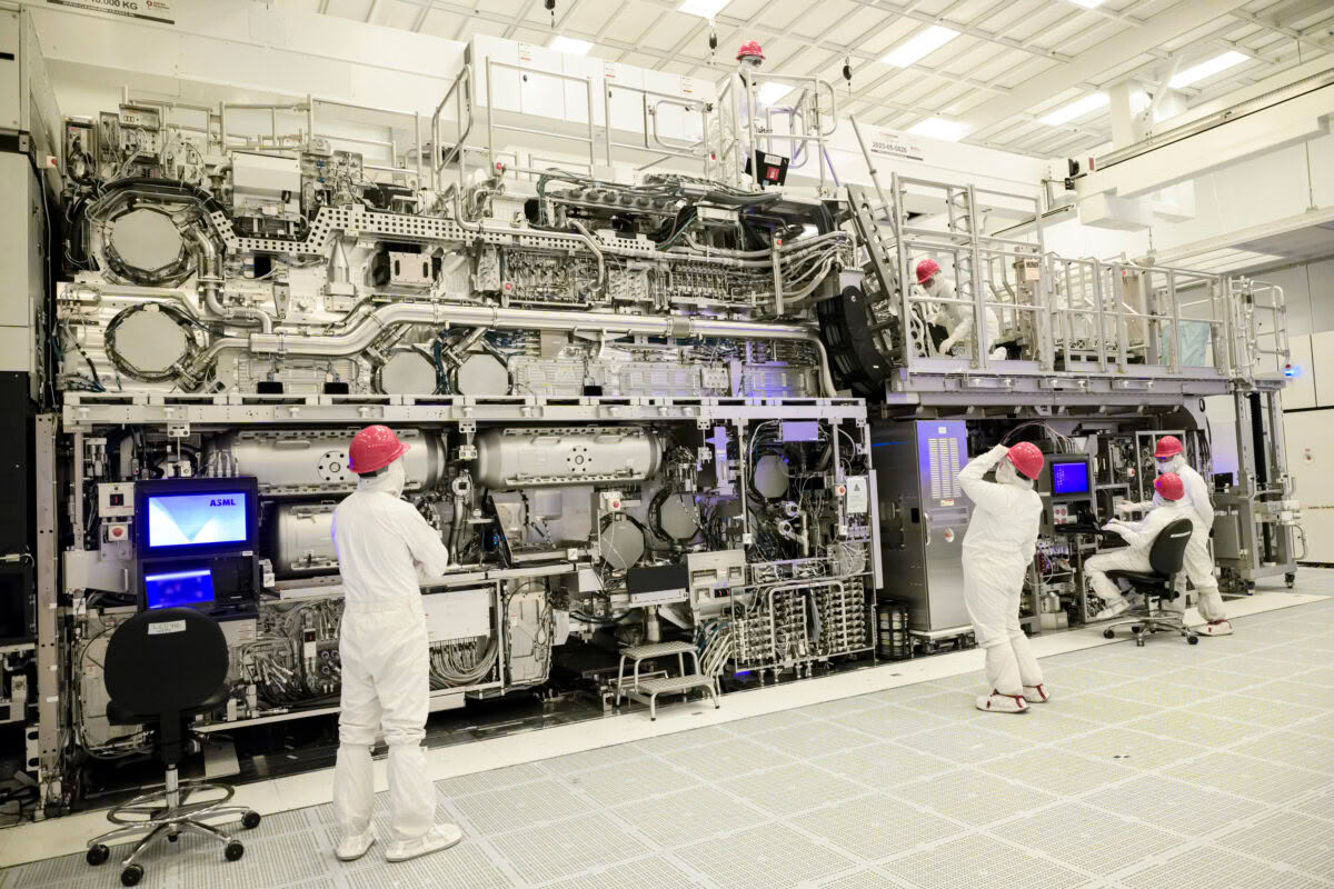
The higher resolution can allow some structures to be printed with a single pattern rather than relying on multiple exposure steps.
That matters because multi patterning increases manufacturing complexity, cost and the possibility of defects.
For sufficiently advanced nodes, High NA EUV could therefore simplify parts of the production process even though the machines themselves are extremely expensive.
Samsung previously expected earlier adoption
Samsung had considered using High NA EUV for its 2nm and 1.4nm technologies.
The company now appears to believe that conventional EUV can remain useful for longer than previously expected.
Samsung’s technology leadership indicated that High NA systems are more likely to become necessary from the 1nm generation onward.
That means the company can continue refining existing lithography approaches for earlier nodes rather than introducing a major new manufacturing platform too soon.
TSMC is also taking a cautious approach
Samsung is not alone in delaying widespread use of High NA EUV.
TSMC has also reportedly considered alternatives for advanced nodes, including improved photomask pellicles and other process techniques that could allow existing EUV tools to remain useful.
The trend suggests that chipmakers are balancing the technical benefits of High NA EUV against its cost and maturity.
Intel has moved more aggressively and installed one of the first commercial High NA EUV systems at its Oregon development facilities.
Samsung and TSMC appear more willing to wait until the technology provides a clearer production advantage.
High NA may become more important at 1nm
The main argument for High NA EUV strengthens as process nodes continue shrinking.
At larger nodes, manufacturers may be able to use conventional EUV with additional patterning steps.
At around 1nm, however, those techniques become increasingly difficult and expensive.
High NA EUV could reduce the number of patterning steps needed while improving the ability to print smaller features directly.
That is why Samsung now expects the technology to become necessary from its A10 generation and beyond.
Cost remains an important factor
High NA EUV systems are among the most expensive pieces of semiconductor manufacturing equipment available.
Introducing them requires more than buying the machines. Chipmakers also need new process flows, supporting infrastructure, masks, metrology and production tuning.
Delaying adoption allows Samsung to avoid some of those costs until the technology is more mature and its benefits are harder to replace with existing methods.
The shift does not mean Samsung is abandoning High NA EUV.
Instead, the company appears to be reserving the technology for the point where conventional EUV becomes less practical.
If current plans hold, that transition could happen around the 1nm generation near 2030, putting Samsung alongside other major foundries that are taking a gradual approach to ASML’s next generation lithography platform.


Discussion (0)
Be the first to comment.