



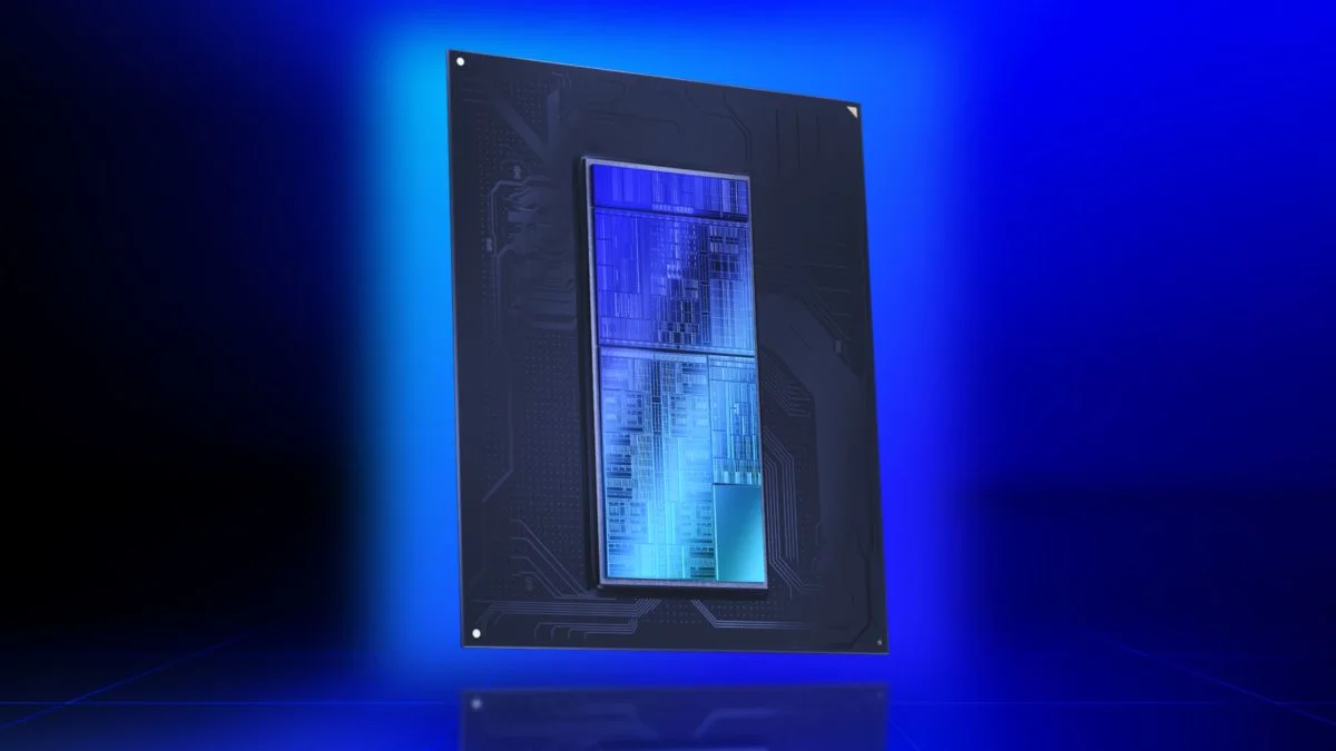
Intel has started using ASML’s High NA EUV lithography technology in production for selected layers of its Panther Lake processors, marking an important step for both companies.
The chips are being manufactured on Intel’s advanced 18A process. ASML describes Panther Lake as the first high volume logic product to use High NA EUV, although Intel is applying the technology only to a subset of layers rather than the entire processor.
Intel installed its first High NA EUV system at its research and development facility in Hillsboro, Oregon, in 2024. The company became the first chipmaker to install and complete acceptance testing of ASML’s second generation TWINSCAN EXE:5200B system.
The equipment has now moved beyond testing and development. Selected Intel 18A layers have been qualified for production using High NA EUV, while the resulting process is said to deliver yields comparable with ASML’s existing NXE EUV platform.
High NA EUV can print smaller and denser chip features
Extreme ultraviolet lithography is used to transfer extremely small circuit patterns onto silicon wafers. The technology allows semiconductor manufacturers to create smaller transistors and fit more components into a limited area.
High NA EUV increases the numerical aperture of the optical system, allowing the equipment to print finer patterns than conventional EUV machines.
| Technology detail | Intel and ASML implementation |
|---|---|
| Lithography platform | ASML TWINSCAN EXE:5200B |
| Manufacturing process | Intel 18A |
| First product | Selected Panther Lake processors |
| Production location | Hillsboro, Oregon |
| Current use | Selected chip layers |
| Production status | High volume manufacturing |
| Yield position | Comparable with existing NXE systems |
| Main benefit | Finer and denser patterning |
The improved resolution could reduce the need for some complex patterning techniques that require several manufacturing steps. Fewer steps may improve production efficiency, although High NA systems are expensive and require significant changes to factory equipment and processes.
Intel is using the technology as an additional manufacturing option. Existing EUV machines remain part of the 18A production flow, while High NA EUV is used where its higher resolution provides a clear advantage.
Panther Lake becomes the first commercial test of High NA production
Panther Lake is expected to form part of Intel’s Core Ultra Series 3 processor family. The chips are designed for laptops and other mobile systems and are among the first products built with the company’s 18A technology.
Intel says only selected Panther Lake layers use High NA EUV. This controlled introduction allows the company to gain manufacturing experience without depending on the new equipment for every part of the chip.
That approach also gives Intel time to evaluate production output, reliability, costs, and yield performance before expanding High NA EUV to more layers or future process nodes.

ASML says the milestone demonstrates that its EXE platform is mature enough for commercial logic production. The company expects other semiconductor manufacturers to decide when and where High NA EUV should enter their own production processes.
The needs of each manufacturer will differ. Some may adopt it quickly for the most difficult layers, while others may continue using conventional EUV with multiple patterning until the cost and production advantages become clearer.
Intel gains an early manufacturing advantage over its rivals
Intel is the first major semiconductor manufacturer to bring High NA EUV into volume logic production.
TSMC is reportedly considering wider adoption closer to 2029, while other manufacturers are also evaluating the technology for future nodes. This gives Intel early experience with the equipment, production methods, materials, and design rules required to use High NA EUV effectively.
The advantage does not guarantee that Intel 18A will outperform rival processes. Chip manufacturing depends on several factors, including transistor design, yield, power efficiency, density, packaging, and production cost.
However, early access gives Intel more time to solve practical problems and build knowledge before High NA EUV becomes more common across the industry.
The company can also use that experience to support external customers through Intel Foundry. Customers may value access to advanced lithography if it improves density or reduces the number of processing steps needed for difficult designs.
High NA EUV could play a larger role in future Intel nodes
Intel’s current use of the technology is limited, but it creates a foundation for wider adoption.
Future processors, AI accelerators, and foundry products will require smaller features and more complex designs. High NA EUV could help manufacturers continue increasing transistor density when older lithography methods become too difficult or expensive.
The machines are physically large and costly, and integrating them into a factory requires new masks, materials, inspection tools, and production methods. Their value will depend on whether they can improve output and reduce manufacturing complexity enough to justify those costs.
For now, Panther Lake provides the first commercial proof that High NA EUV can be used in high volume logic manufacturing. Intel’s decision to apply it to selected 18A layers limits the immediate risk while giving the company real production experience.
The milestone is important for ASML as well. Its High NA systems are moving from research installations into active chip manufacturing, creating a path toward wider use on future semiconductor processes.


Discussion (0)
Be the first to comment.