



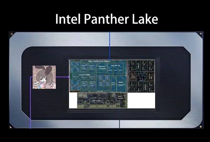
New high resolution die photographs have provided a detailed look at Intel’s Panther Lake compute tile, offering a clear view of the structures inside the company’s latest Core Ultra Series 3 laptop processors.
The images were captured from uncut processor wafers shown at Computex 2026, rather than by physically delidding or chemically stripping retail chips. That approach allowed the silicon structures to be photographed directly using a macro lens.
The Panther Lake compute tile is manufactured on Intel’s 18A process, and the dense layout makes the images especially interesting because several major CPU structures can still be identified clearly.
| Panther Lake element | What can be seen |
|---|---|
| Process node | Intel 18A |
| P cores | Cougar Cove |
| E cores | Darkmont |
| Low power cores | Separate low power cluster |
| Media engine | Integrated on compute tile |
| Display engine | Integrated on compute tile |
| Xe3 graphics | Located on a separate die |
| Product family | Core Ultra Series 3 laptops |
Panther Lake’s 18A compute tile is clearly visible
The die images focus on the compute tile used in Intel’s mainstream Panther Lake processors.
These chips form part of the Core Ultra Series 3 laptop family and use Intel’s 18A manufacturing technology.
The photographer noted that the high density of 18A silicon made the die more difficult to capture than some of Intel’s other recent processors.
Even so, the larger structures remain visible enough to identify several important blocks.
The most obvious are the Cougar Cove performance cores and the quad core clusters of Darkmont efficiency cores.
Cougar Cove and Darkmont cores can be picked out
The images make Intel’s hybrid CPU layout easier to understand visually.
Large Cougar Cove P cores occupy distinct areas of the tile, while the Darkmont E cores are grouped into compact four core clusters.
A separate low power core cluster is also visible away from the main CPU structures.
That physical separation reflects Intel’s continued focus on power management and background task efficiency in mobile processors.
Seeing these blocks directly in silicon provides a more concrete picture of how Panther Lake divides workloads between performance, efficiency, and low power processing resources.
Media and display engines remain on the compute tile
One of the more interesting design choices visible in the die is the placement of the media and display engines.
Both remain integrated into the compute tile even though Panther Lake’s Xe3 graphics hardware is located on a separate die.
The reason given is power management.
Keeping display and media functions on the compute tile allows the system to handle certain tasks without needing to wake the full graphics tile.
That can reduce unnecessary power use during video playback, display output, and other lighter workloads.
Xe3 graphics sit on a separate die
Panther Lake continues Intel’s tiled processor design rather than putting every major component onto one piece of silicon.
The actual Xe3 GPU hardware is located elsewhere in the package.
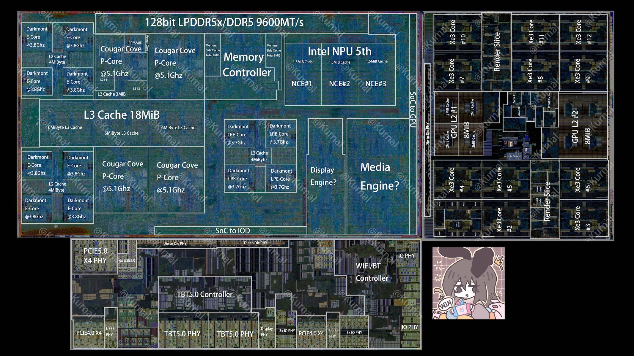
The die images therefore show only the compute side of the design, not the graphics architecture itself.
This separation allows Intel to optimize different parts of the processor independently while also using different layouts for power and performance management.
Intel showed multiple processor wafers at Computex
The Panther Lake images were not the only die photographs produced from Intel’s Computex display.
The photographer also captured wafers for several other recent Intel processors, including Wildcat Lake, Clearwater Forest, Granite Rapids, and Sierra Forest.
The supplied report focuses primarily on Panther Lake, but those additional images provide similar visual insight into Intel’s broader processor portfolio.
The photographs are notable because they were taken directly from exposed wafers rather than through the more complicated process normally required to reveal a packaged processor die.
Die photography makes CPU architecture easier to understand
Processor block diagrams can explain where cores, caches, engines, and other logic are located, but physical die photographs show how much silicon those components actually occupy.
In Panther Lake’s case, the images make it easier to see the relative scale of the P cores, E core clusters, low power cores, and supporting logic.
They also highlight Intel’s increasingly modular approach to processor design.
The 18A compute tile carries the CPU, media, and display functions, while Xe3 graphics live on another die within the same package.
That physical layout helps explain how Intel is balancing performance and efficiency in its latest mobile processors.
The new images do not reveal new specifications, but they provide one of the clearest visual looks yet at how Panther Lake’s 18A silicon is physically organized.


Discussion (0)
Be the first to comment.