




Intel has moved the production schedule for its 14A semiconductor process forward, with risk production on internal products now planned for the second half of 2027 and high volume manufacturing expected to begin in 2028.
The revised timeline brings the high volume ramp forward by roughly one year compared with Intel’s earlier 2029 target. CEO Lip-Bu Tan said the company has become increasingly confident that 14A can compete across performance, power efficiency, transistor density, cost and production schedule.
Intel is currently developing the process for both its own future chips and external foundry customers. The company has not identified the major customers evaluating 14A, but it says engagement is increasing as the technology moves closer to production.
The schedule remains dependent on manufacturing yields, design readiness and customer commitments. Risk production is an important milestone, but it does not guarantee that large commercial volumes will follow without further technical and operational progress.
| Intel process milestone | Current schedule |
|---|---|
| 14A PDK 0.5 | Already available |
| 14A PDK 0.9 | Expected in October 2026 |
| Internal risk production | Second half of 2027 |
| High volume production | 2028 |
| Previous high volume target | 2029 |
| 18A-P risk production | Already started |
Intel says 14A is progressing faster than 18A did at a similar stage
Intel claims that 14A is performing better than its 18A process did at the same point in development.
The company says the newer node is ahead in both defect density and transistor performance. Defect density measures the number of manufacturing flaws found across a given area of silicon and is an important indicator of potential chip yields.
Lower defect density generally means that a larger percentage of chips produced on each wafer can meet their required specifications. This can reduce manufacturing costs and make the process more attractive to external customers.
Transistor performance is equally important because it affects the speed and power efficiency of chips manufactured on the node.
Intel’s confidence is also based on the progress of its process design kits. These kits provide chip designers with the models, rules and tools required to create products for a manufacturing process.
PDK 0.5 is already available, while PDK 0.9 remains on schedule for October 2026. A later and more complete design kit should allow customers to move closer to final product designs.
Intel is also building and validating the supporting intellectual property required for 14A, including memory interfaces, interconnects and other reusable chip components.
Internal products will lead the first 14A production phase
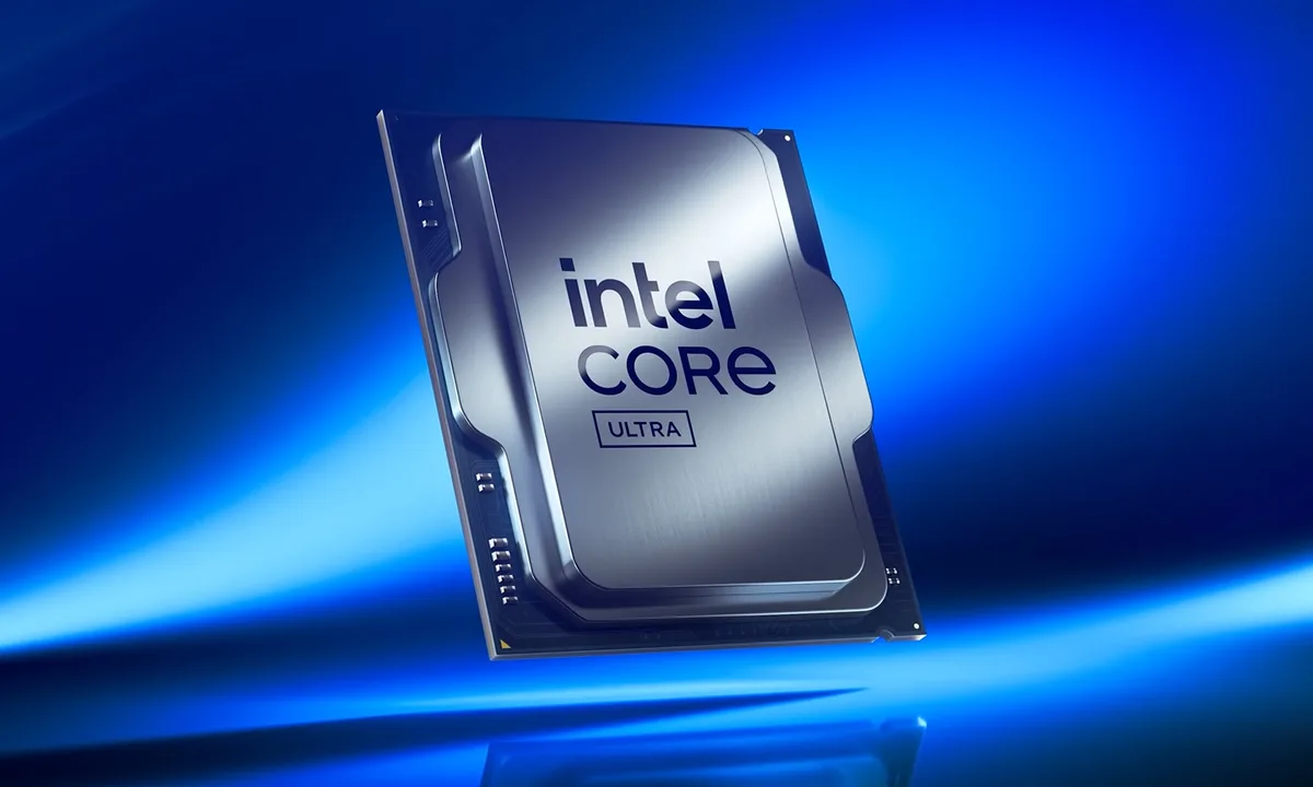
Intel plans to begin risk production using its own products during the second half of 2027.
Risk production involves manufacturing early versions of a chip before the process reaches full commercial maturity. It allows engineers to identify remaining problems in yields, performance and design rules before larger volumes are produced.
Using internal products gives Intel greater control over the first ramp. Its product teams can work directly with the foundry organisation to resolve manufacturing and design issues.
These early chips will also act as demonstrations for potential foundry customers.
External customers are unlikely to commit major products to a new node unless Intel can prove that the process works at scale and delivers competitive performance, power and cost.
The company has not confirmed which internal product families will use 14A first. Their launch timing, market position and technical results will play an important role in shaping customer confidence.
Progress on Intel 18A is supporting the company’s broader foundry plan
Intel also reported improved output across Intel 7, Intel 3 and Intel 18A during the second quarter.
The company said these processes exceeded internal volume targets because of better equipment use, shorter production cycles and higher wafer availability.
Intel 18A output has increased as the company prepares to ramp products including Panther Lake and Wildcat Lake.
Panther Lake is associated with the Core Ultra Series 3 family, while Wildcat Lake is expected to appear under the Core Series 3 branding.
Intel has also started risk production on 18A-P, an improved version of the 18A node.
The performance of 18A remains important for 14A because it will show whether Intel can execute a major process transition on time and at competitive yields.
Customers considering 14A will closely examine how smoothly Intel handles the 18A ramp. Strong results could improve confidence, while delays or yield problems could make customers more cautious.
14A will introduce additional manufacturing technologies
Intel’s roadmap positions 14A as a major step beyond 18A.
The process is expected to use High Numerical Aperture extreme ultraviolet lithography, often called High-NA EUV. This technology can print smaller and more detailed features than current EUV systems.
Intel also plans to use its PowerDirect technology, an evolution of the company’s backside power delivery approach.
Backside power delivery moves some of the power connections away from the front of the chip. This can free space for signal wiring and potentially improve power efficiency and transistor density.
These technologies may help Intel compete with advanced nodes from TSMC and Samsung.
They also introduce manufacturing complexity. High-NA EUV tools are expensive, require new production processes and must be integrated carefully into the manufacturing flow.
Intel will need to show that these additions improve chip performance and economics without creating unacceptable yield problems.
External customer interest will determine the commercial value of 14A
Intel says customer engagement around 14A is increasing, but it has not announced the major companies involved.
The foundry business needs external customers to justify the cost of developing and operating advanced manufacturing nodes.
A leading process requires billions of dollars in research, equipment and factory capacity. Intel cannot rely only on its own processors if it wants the foundry operation to compete at global scale.
Large customers could provide stable wafer demand and help spread development costs across more products.
However, chip designers need confidence in Intel’s manufacturing schedule, design tools, yields and ability to protect confidential information.
They must also decide whether moving from established foundries is worth the cost and risk of redesigning products for Intel’s process.
The earlier 2028 production target suggests that Intel believes there is enough internal and external demand to support a faster ramp.
Intel still faces a difficult execution test
Moving the schedule forward is a positive sign, but the most important work remains ahead.
Intel must complete the process design kit, finalise supporting intellectual property, improve yields and bring internal chips through risk production.
It must then scale manufacturing without losing control of cost, cycle time or quality.
The company also needs to convince external customers that its roadmap is reliable after years of delays across earlier process generations.
Intel’s recent manufacturing improvements provide some evidence of progress, but 14A will be judged by production results rather than development claims.
The company has now committed to a 2028 high volume ramp. Meeting that target would strengthen Intel Foundry’s position and give chip designers another advanced manufacturing option alongside TSMC and Samsung.


Discussion (0)
Be the first to comment.