



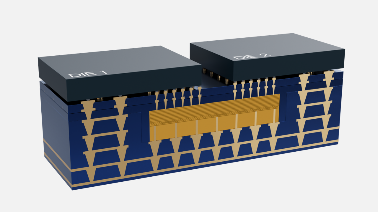
Intel is developing extremely large processor packages that could reach 240mm by 240mm, allowing future AI and high performance computing systems to combine many specialised chiplets within one design.
The company calls the concept Hyper Large Form Factor packaging. Its research targets packages up to 24 times the size of a standard reticle, with longer term plans moving beyond that level through panel based manufacturing.
Intel says its advanced packaging facility in Rio Rancho, New Mexico, has already validated several large EMIB and Foveros designs. An important part of this work involved solving encapsulation problems that become increasingly difficult as packages grow.
The technology is not yet a finished commercial product. However, Intel’s tests suggest that several technical barriers to building much larger chip packages can be addressed through new materials, assembly methods, power delivery and cooling systems.
| Development area | Reported target |
|---|---|
| Maximum package concept | 240mm by 240mm |
| Reticle scale | Up to 24 times standard size |
| Near term roadmap | Beyond 12 times by 2028 |
| Longer term direction | Above 50 times through panel packaging |
| Expected power range | 15kW to 25kW |
| Main packaging methods | EMIB, EMIB T and Foveros |
Large chiplet systems are replacing single die processors
Modern processors increasingly combine several smaller silicon dies rather than relying on one large piece of silicon.
These chiplets can perform different tasks, including general processing, graphics, artificial intelligence, memory control and networking. Advanced packaging connects them so they can operate as one system.
This approach improves manufacturing flexibility because each chiplet can use a process technology suited to its purpose. It can also reduce waste because smaller dies are generally easier to manufacture successfully than one very large die.
The challenge is that package size and connection density create new limits. As more chiplets are added, data must travel farther, power delivery becomes more difficult and the complete package becomes harder to manufacture without defects.
Intel is using EMIB bridges and Foveros stacking to overcome some of these limits. EMIB provides dense connections between chiplets, while Foveros allows dies to be placed vertically.
Intel targets packages far larger than current designs
Intel’s Hyper Large Form Factor research aims to expand packages well beyond the sizes used in today’s processors.
Current work at the Rio Rancho facility supports designs around eight times the standard reticle area. Intel expects to move beyond 12 times by 2028, while its broader research explores packages reaching 24 times.
A 24 times reticle design could measure approximately 240mm on each side. Such a package would be closer in size to a small circuit board than a conventional processor.
These designs are intended for systems that require large numbers of compute and memory chiplets. AI accelerators are a likely use because they need substantial processing capacity and high bandwidth memory within the same package.
Data connections must reach much higher speeds
Moving information quickly between chiplets is one of the main challenges in a large package.
Intel’s EMIB T bridges use metal layers with features smaller than two micrometres. The company is targeting data rates of 64Gbps per channel for chip to chip and chip to memory communication.
Connections leaving the package will require even higher performance. Intel is evaluating co packaged copper cables and optical links for projected speeds of up to 448Gbps.
Copper may remain useful for shorter connections, while optical technology could provide better efficiency when data must travel farther.
| Connection type | Reported target |
|---|---|
| Internal chiplet connection | 64Gbps per channel |
| Future external connection | Up to 448Gbps |
| Internal bridge technology | EMIB T |
| External options | Co packaged copper and optics |
These speeds are necessary because adding more processors is only useful if they can exchange data without creating delays.
Power delivery becomes more difficult at larger scales
Traditional processor packages often deliver power from connections around the package edges.
That approach becomes less efficient as package dimensions increase. Components near the centre may be far from the external power connections, increasing resistance and making voltage stability harder to maintain.
Intel proposes placing silicon capacitors within the substrate and directly beneath the processor dies. These capacitors could provide as much as one millifarad of local energy storage for each full reticle area.
The company is also studying voltage regulators placed on or inside the package. Bringing these components closer to the chiplets could allow faster responses when power requirements change.
This will be important because future Hyper Large Form Factor packages could consume between 15kW and 25kW. That is far beyond the power draw of conventional consumer processors.
Redundant connections could improve manufacturing yield
A package containing many chiplets and communication links has more opportunities for a defect to occur.
Intel proposes adding spare data lanes beside the active connections. If one lane fails during manufacturing, another could take its place.
Adding three or four spare lanes to a group of 64 could reportedly increase connection bundle yield from about 97 percent to more than 99 percent.
That difference may appear small, but it becomes financially important when a single package includes many groups of connections and expensive processor dies.
Without redundancy, one faulty lane could make a large and costly package unusable.
Warping is a major physical challenge
Large packages can bend or warp as different materials expand and contract at different rates.
Intel’s modelling found that a free standing Hyper Large Form Factor package could warp by as much as 7mm at room temperature. That would be enough to affect electrical connections and prevent cooling hardware from making proper contact.
The proposed solution combines thick stiffener rings, glass core substrates with low expansion and a solder process using several ball sizes.
Intel also expects the cooling assembly to apply more than 4,500 newtons of pressure during operation. This force would help keep the package close to flat.
Glass substrates may become especially important because they can offer better dimensional stability than conventional organic materials.
Cooling systems may need independent thermal zones
Removing heat from a package consuming up to 25kW cannot be handled by a simple processor cooler.
Intel proposes a modular cooling structure divided into cells. Each section would have its own sensors and thermal controls, allowing cooling power to be directed where it is needed.
Individual modules are expected to support more than 5kW of cooling capacity. Several modules could then work together across the complete package.
This design would be more flexible than placing one large cold plate over the entire system. It could also respond better to local hot spots created by different processor and memory chiplets.
Intel solves a difficult encapsulation problem
Encapsulation protects the chiplets and the connections beneath them. An underfill material flows into the small spaces between the dies and substrate before being cured.
As packages become larger, the underfill must travel farther. Longer distances increase resistance and make it harder to remove trapped air, which can create voids and reliability problems.
Current underfill flow distances are around 43mm for some EMIB designs and roughly 22mm for conventional packages. Hyper Large Form Factor systems require much greater coverage.
Intel addressed the problem through three coordinated changes.
First, it developed a lower viscosity underfill that can travel farther without losing mechanical reliability. Second, it changed from applying the material mainly at the edges to dispensing it from several points. This reduces the distance the material must travel.
Finally, Intel adjusted the curing process so that remaining voids collapse before the material hardens.
Early test packages achieved void free results
Intel says it validated an EMIB package larger than five times the standard reticle area.
The test design included 18 dies and space for 12 high bandwidth memory stacks. It achieved void free encapsulation with underfill flow distances reaching 40mm.
A tiled EMIB package larger than seven times the reticle area also produced void free results.
With Foveros packaging, Intel achieved void free encapsulation at two times and four times reticle scales. The smaller two times design also completed full reliability testing.
These tests show that Intel can build large experimental packages, but the company still needs to increase manufacturing scale and demonstrate commercial yields.
Intel plans to continue expanding beyond seven times reticle size, with designs above 12 times expected in the near term. Panel level packaging could eventually move beyond 50 times the standard reticle area.
The Rio Rancho facility will be central to that work. Intel is positioning the site as a major US centre for advanced packaging and the development of extremely large chiplet based systems.

Discussion (0)
Be the first to comment.