



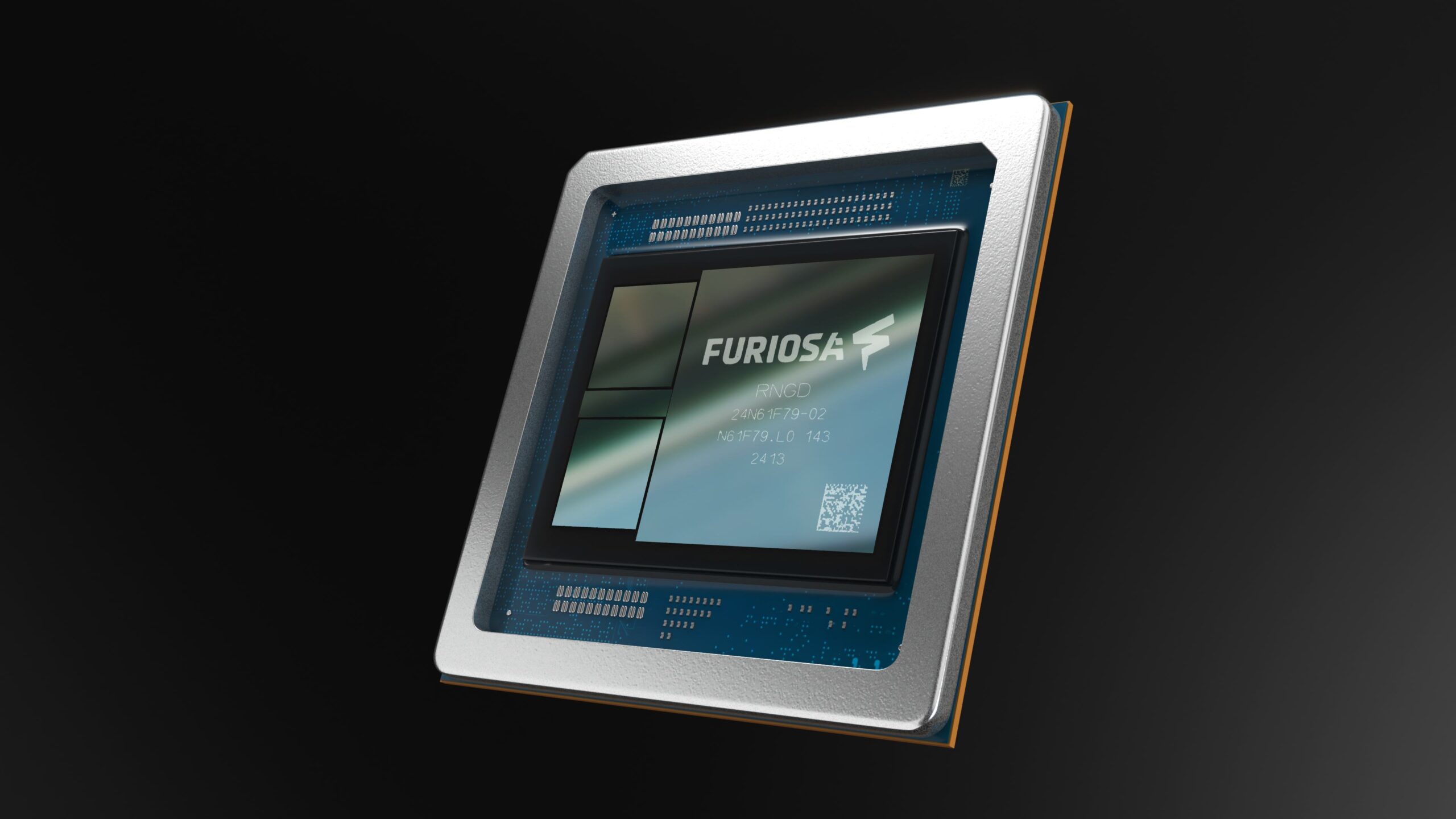
FuriosaAI is taking a different path from traditional GPU based AI acceleration with its next generation inference chip. The company has announced a third generation AI accelerator built with Broadcom, using a 2nm chiplet design and next generation HBM4 or HBM4E memory. The goal is to improve AI inference performance by focusing heavily on memory bandwidth, data movement, and rack scale deployment rather than following the normal GPU playbook.
The new accelerator will build on FuriosaAI’s current RNGD platform, which is already in mass production on TSMC’s 5nm process. That second generation chip is a 180W PCIe design aimed at large language model and agentic AI workloads. The third generation design goes further by targeting the growing demand for inference, where companies need to serve large AI models quickly and efficiently at scale.
FuriosaAI is betting that AI inference needs bandwidth first, not just more GPU power
The most important detail is the memory setup. FuriosaAI says the new platform will pair a 2nm compute die with HBM4 or HBM4E memory. The teaser image reportedly shows 12 HBM memory sites, two large compute chiplets, and two I O controllers. If the company uses 12 high 36GB HBM stacks, the chip could reach 432GB of high bandwidth memory.
That kind of memory capacity and bandwidth could matter a lot for inference workloads. Modern AI systems are not only limited by raw compute. They also need to move huge amounts of data quickly while keeping latency low. FuriosaAI claims its architecture can deliver higher performance per watt and greater token density than even efficient GPU designs by focusing on bandwidth and tensor contraction processing.
| Area | FuriosaAI third generation accelerator |
|---|---|
| Manufacturing target | 2nm compute technology |
| Partner | Broadcom |
| Memory | HBM4 or HBM4E |
| Possible memory setup | 12 HBM sites, potentially up to 432GB |
| Main workload | AI inference and agentic AI |
| Current platform | RNGD, built on TSMC 5nm |
| Sampling target | First half of 2028 |
Broadcom’s role is important. FuriosaAI will use Broadcom’s advanced packaging capabilities to integrate multiple silicon dies into one high performance AI chip. The company will also use Broadcom’s Ethernet and PCIe technologies for high bandwidth networking across large AI clusters.
That suggests FuriosaAI is not only trying to build a single fast chip. It wants a platform that can scale across data center racks. That is important because the next stage of AI infrastructure is increasingly about serving huge numbers of tokens across many models, agents, and enterprise workloads.
The company also says its software stack is designed to make deployment easier. Furiosa’s SDK uses a compiler that maps high level PyTorch code to its silicon. For developers who want more control, Furiosa also offers a Virtual ISA with a declarative programming model. The idea is to provide hardware control without the same complexity often associated with GPU programming.
This is still a future product, not something enterprises can deploy today. FuriosaAI expects the third generation accelerator to begin sampling in the first half of 2028. That means the market may look very different by the time it arrives, especially with Nvidia, AMD, Intel, and custom silicon providers all pushing aggressively into AI inference.
Still, the announcement shows where AI hardware is heading. As inference demand rises, memory bandwidth, power efficiency, and cluster scale networking may become just as important as raw compute. FuriosaAI is betting that a purpose built inference chip with HBM4 class bandwidth can compete with GPUs by solving the bottlenecks that matter most for large AI deployments.


Discussion (0)
Be the first to comment.