



ASML, TSMC, and Samsung are backing a transition to much larger 12 inch photomasks as the semiconductor industry prepares for wider use of High NA EUV lithography.
The change is intended to solve a major limitation created by High NA EUV's smaller exposure field. With current 6 inch photomasks, very large chips such as AI accelerators may need to be split across multiple exposures and stitched together during manufacturing.
A larger mask format could reduce that complexity and improve throughput as chipmakers move toward more advanced process nodes.
| Detail | Current plan |
|---|---|
| Lithography technology | High NA EUV |
| Current photomask size | 6 inches |
| Proposed photomask size | 12 inches |
| High NA aperture | 0.55 |
| Conventional EUV aperture | 0.33 |
| Samsung volume deployment | Planned from 2028 |
| TSMC volume deployment | Planned from 2030 |
| 12 inch mask pilot line | Targeted for 2031 |
| Full production readiness | Targeted for 2033 |
High NA EUV Improves Resolution but Shrinks the Exposure Field
High NA EUV is designed to print smaller circuit features than today's mainstream EUV systems.
ASML achieves this by increasing the numerical aperture from 0.33 to 0.55.
The higher aperture improves optical resolution, helping chipmakers continue shrinking transistor features at future process nodes.
However, this creates another engineering problem.
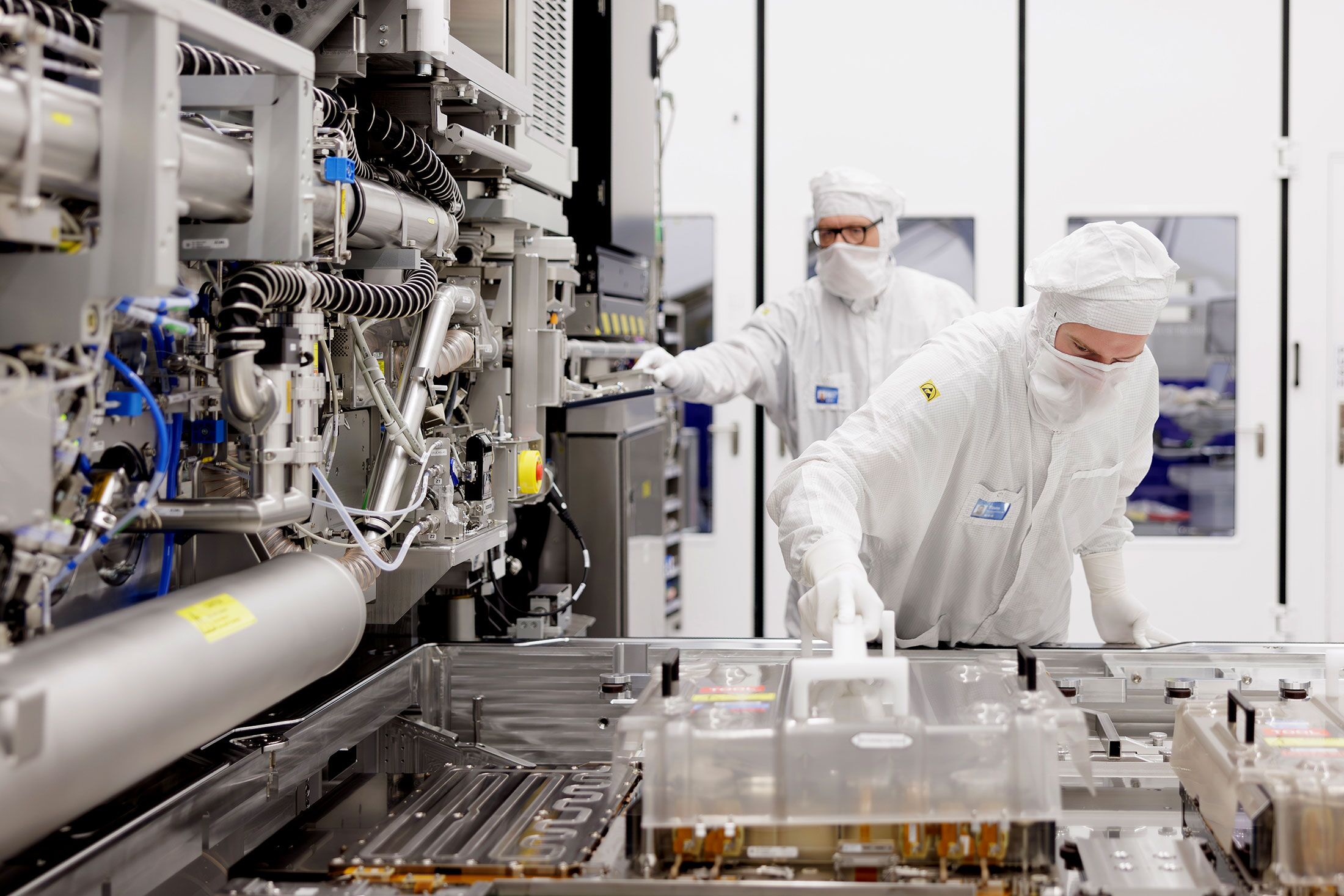
High NA systems use anamorphic optics to control the extreme angles at which EUV light travels through the optical system.
That design reduces the usable exposure field on the wafer by roughly half compared with conventional EUV.
For smaller chips, that may not be a major problem.
For large processors, especially AI accelerators, the reduced field can become a serious manufacturing constraint.
Large AI Chips May Need Multiple Masks
With today's 6 inch photomask format, some large chip designs cannot fit inside a single High NA exposure field.
Manufacturers may therefore need to divide a chip pattern between two masks and expose the wafer in separate sections.
Those sections then have to be aligned using a stitching process.
Stitching increases manufacturing complexity because the two patterns must line up with very high precision.
It can also introduce alignment risks and reduce throughput by requiring additional exposure steps.
Moving to a 12 inch photomask could allow larger patterns to be handled more efficiently.
TSMC and ASML Launch a Larger Mask Initiative
TSMC and ASML have formally started an industry initiative aimed at moving High NA EUV toward 12 inch photomasks.
Samsung is also supporting the effort through the Large Size Mask Consortium.
The current roadmap calls for a functional 12 inch mask pilot line by 2031.
High NA lithography systems designed around the larger format are then expected to reach readiness for advanced volume production around 2033.
The transition will require changes across several parts of the semiconductor manufacturing ecosystem, including mask production, inspection, handling, and lithography equipment.
This means the larger format is unlikely to replace existing masks quickly.
Samsung Plans High NA EUV for Advanced DRAM
Samsung plans to introduce High NA EUV into high volume manufacturing from 2028.
The company is expected to use the technology initially for advanced DRAM production.
If that schedule holds, Samsung could become the first major memory manufacturer to deploy High NA EUV at large scale.
Memory makers face increasing pressure to improve density and efficiency as demand grows for AI servers and high bandwidth memory systems.
Higher resolution lithography could help Samsung print increasingly complex memory features without relying as heavily on additional patterning steps.
TSMC Targets High Volume Use From 2030
TSMC plans to introduce High NA EUV into advanced high volume manufacturing starting around 2030.
The company expects the number of layers that benefit from the technology to increase as future chip designs become more complex.
Large AI processors are one of the key workloads driving this need.
As accelerators grow in transistor count and physical size, lithography limitations become more difficult to manage.
High NA EUV could reduce the number of patterning steps needed for some critical layers, although its higher equipment cost remains an important consideration.
High NA EUV Tools Are Extremely Expensive
High NA EUV scanners are significantly more expensive than conventional semiconductor manufacturing equipment.
Estimates place the cost of individual systems above $350 million.
That price has made chipmakers cautious about introducing the technology before it is economically necessary.
Intel has been one of the earliest adopters, while Samsung and TSMC are now laying out more concrete plans for volume production.
The growing demand for AI hardware is adding pressure to adopt higher resolution manufacturing tools despite those costs.
Larger Masks Could Improve High NA Economics
The move to 12 inch photomasks is ultimately about making High NA EUV more practical for large and complex chips.
If larger masks reduce the need for stitching, manufacturers could simplify some exposures, lower alignment risk, and improve wafer throughput.
The transition will still take several years.
Samsung's first High NA manufacturing plans begin before the larger mask format is expected to be ready, while TSMC's initial deployment also comes ahead of the 2031 pilot line target.
That means 6 inch masks and stitching techniques are likely to remain part of early High NA production.
The longer term objective is to have 12 inch mask infrastructure and compatible High NA systems ready for broader advanced manufacturing around 2033.

Discussion (0)
Be the first to comment.